
Given the vast scope of electronics design, we've chosen to focus Quilter's near-term product roadmap on the types of boards our users most frequently create—high-density, high-speed digital designs.
And in the wide world of digital electronics, what better place to cut our AI designer’s teeth than on an Internet of Things (IoT) project? And what more iconic an IoT module than the ESP32?
This project post documents my first Quilter project – a custom ESP32 dev board – designed entirely by Quilter’s AI PCB designer without human touch-ups or modifications.
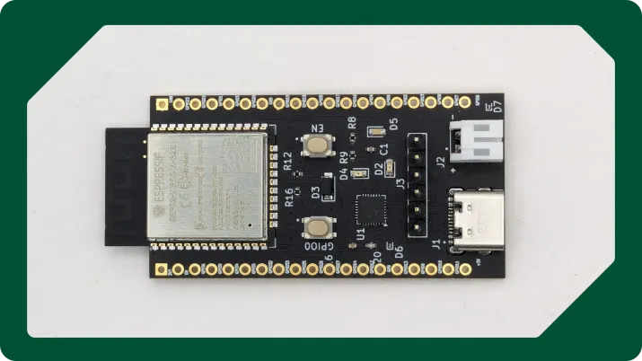
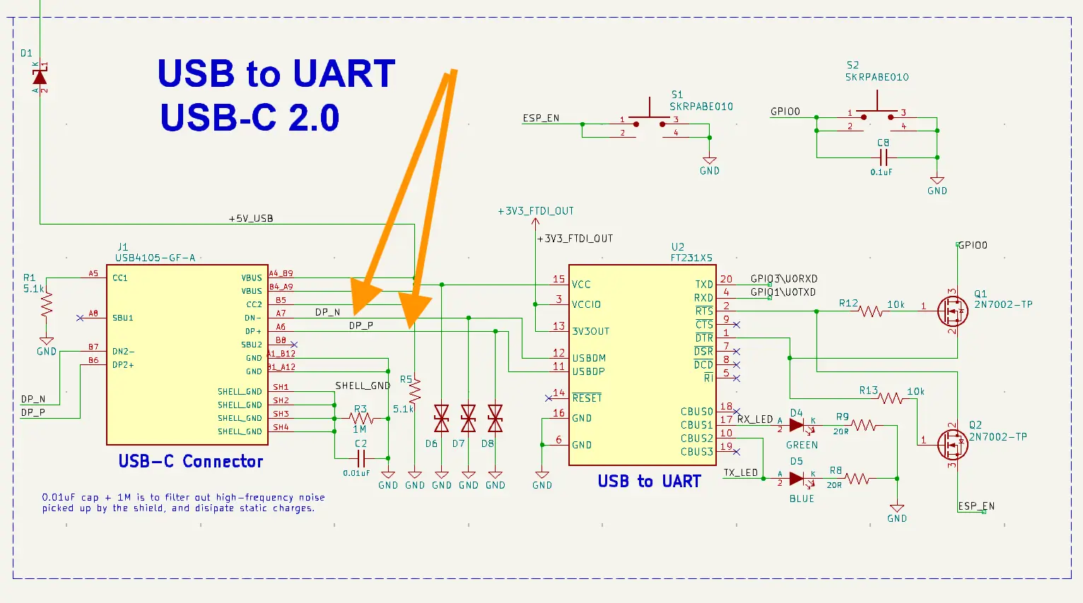
Meet the QSP32, our ESP32-based dev board
The “QSP32” board we built is a perfect example of the type of IoT designs many engineers are focused on today and that Quilter is already well-suited to design.
In particular, this QSP32 design features the ESP32-WROOM-32E module and has:
- plenty of GPIO,
- a USB-to-UART chip,
- and a nifty power IC that manages voltage regulation and battery charging.
The board also includes Boot0 and Reset push buttons and an I2C interface for connecting an external LCD.
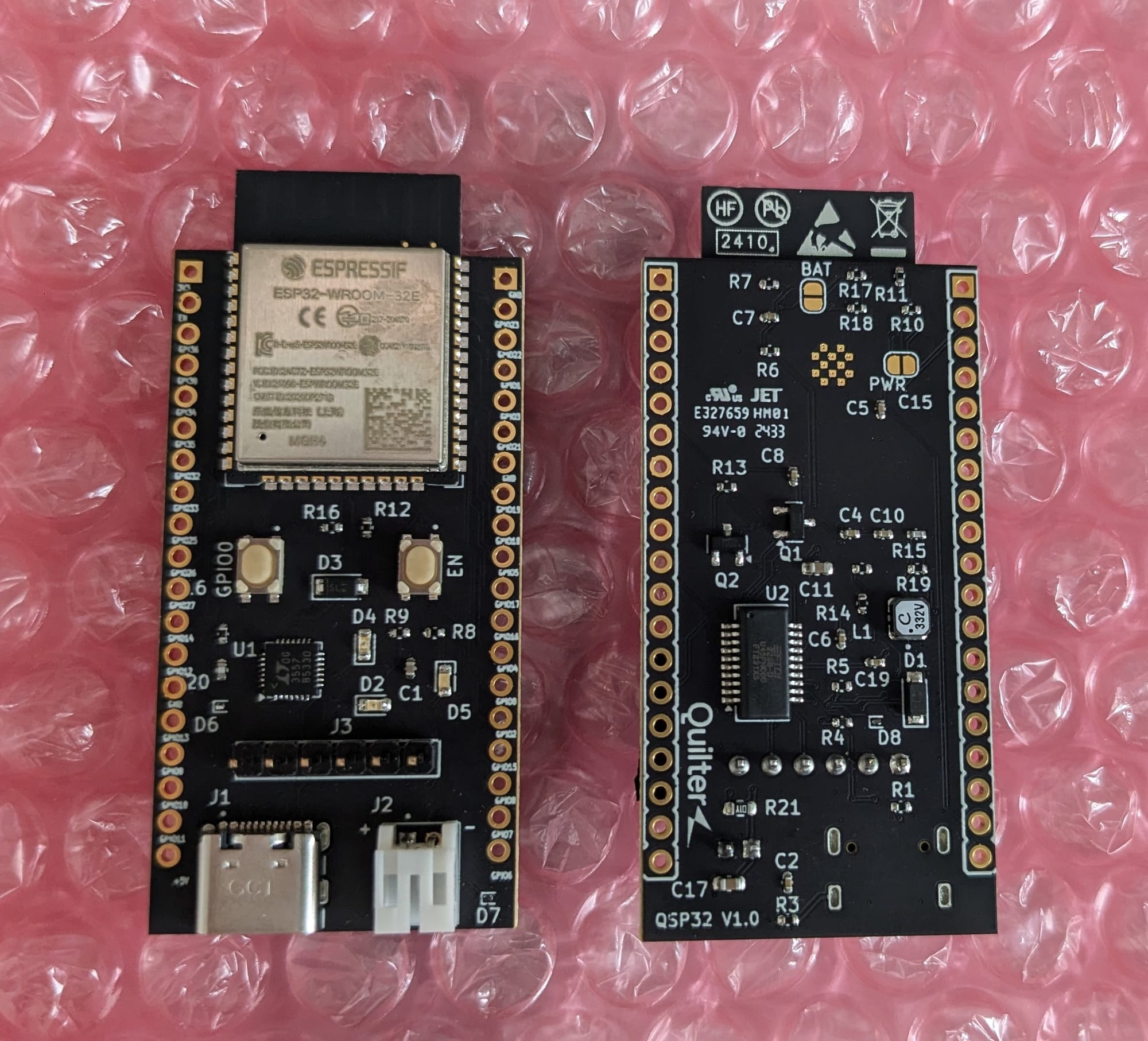
Quilter did a great job with the design; I fabbed it with Macrofab, and it works! 😄
QSP32 flashing an LED via a basic "blinky" Arduino sketch
Designing with Quilter
Configuring a job in Quilter happens in two high-level steps:
- Uploading input files (schematic and board file) that define the netlist, component footprints, board outline, and position of any pre-placed components.
- Defining constraints that identify the primary physics concerns for Quilter’s AI designer to respect during layout.
Input files
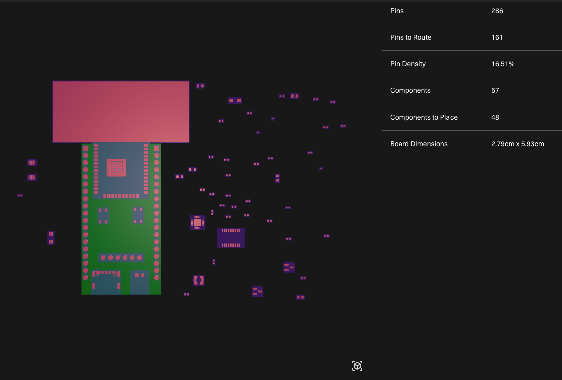
I pre-placed only a handful of location-sensitive components in this design:
- The ESP32 module, because I wanted to ensure the ESP32 trace antenna extends off the edge of the board to reduce signal interference;
- the USB, JST, and header connectors, to ensure they were placed together on a common edge;
- and the push buttons, to ensure they were placed together and symmetrically near the ESP32 module.
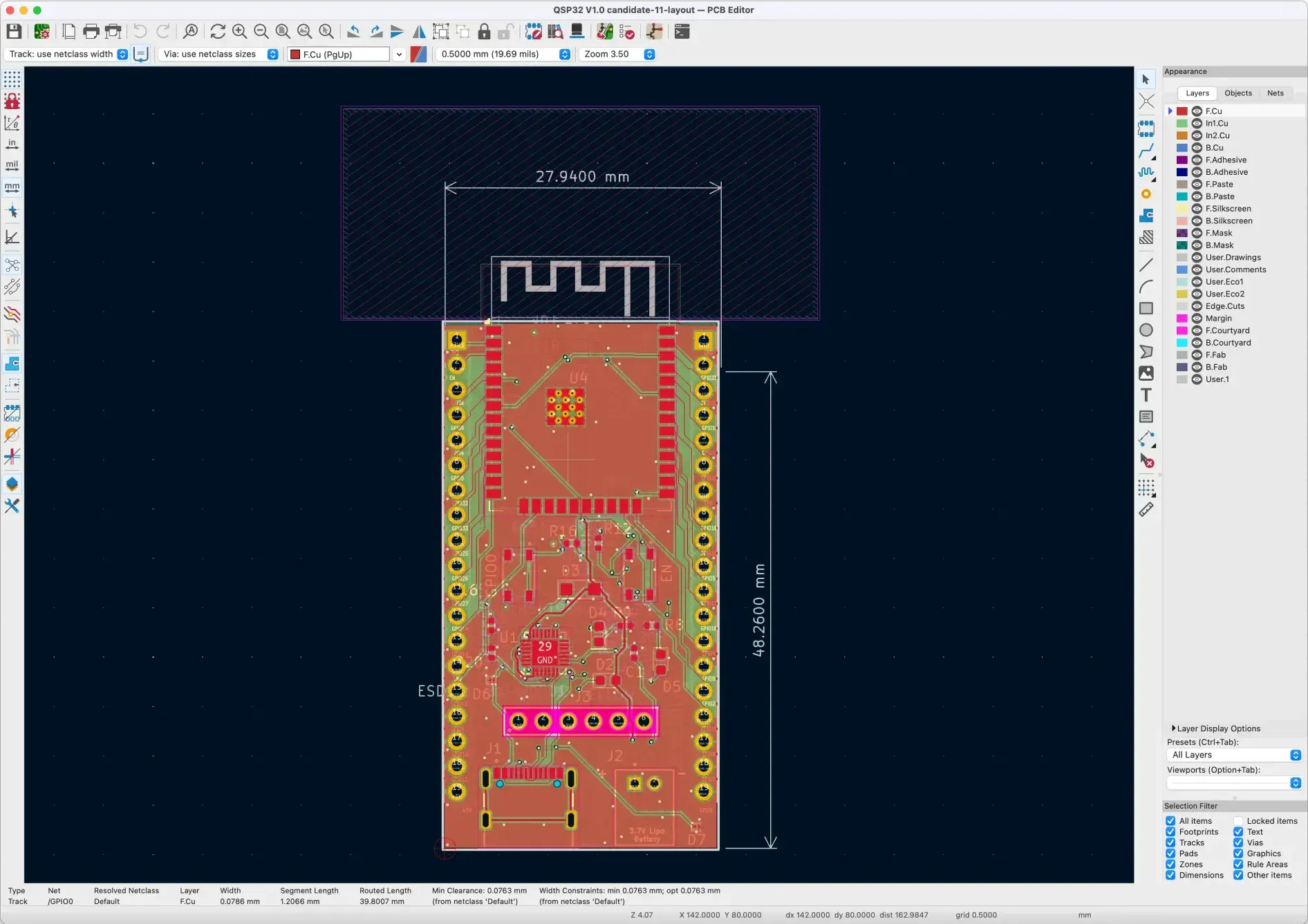
The rest of the components were left unplaced. On the right, you can see that there were 57 components in total – 9 were pre-placed by me, leaving 48 comps with 161 pins left for Quilter to place and route.
Physics constraints
For the QSP32, the primary physics considerations for my designs were:
- High current nets for the USB-C power supply and Li-Po charging circuitry,
- Differential pairs to deliver high-speed USB signals between the USB-C connector and ESP32,
- and Bypass capacitors to ensure adequate decoupling
Stay tuned for my next ESP32-based project – QSP32 Solar Boost – which includes updates to take advantage of both new constraint types!
One reason we selected the ESP32 WROOM module is to avoid the need to consider additional physics constraints like antenna tuning and crystal/load capacitor placement.
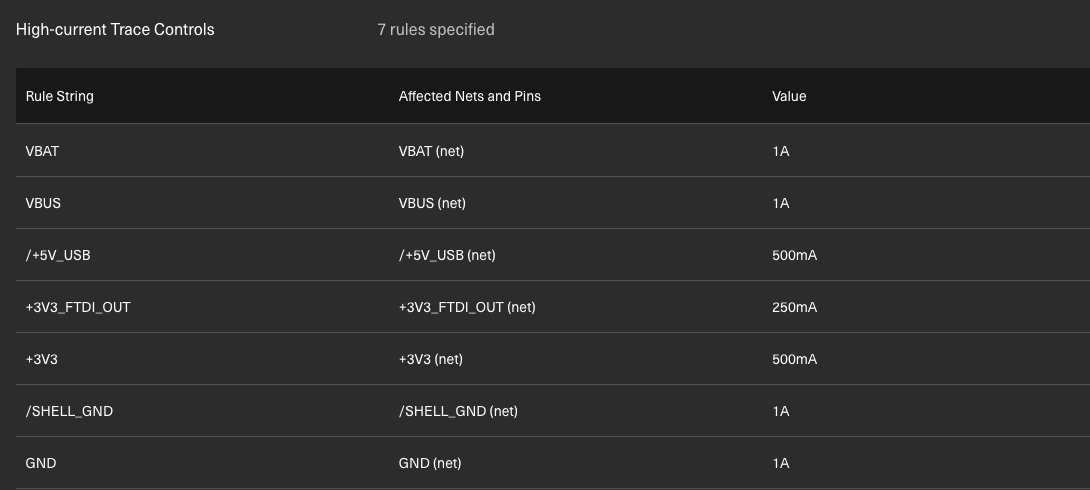
The screenshot below shows the high current net constraints I defined before submitting my layout job to Quilter:
Output file
After an hour and a half of compilation time and 200+ layout candidates later, here’s the design that I ultimately selected for fabrication!
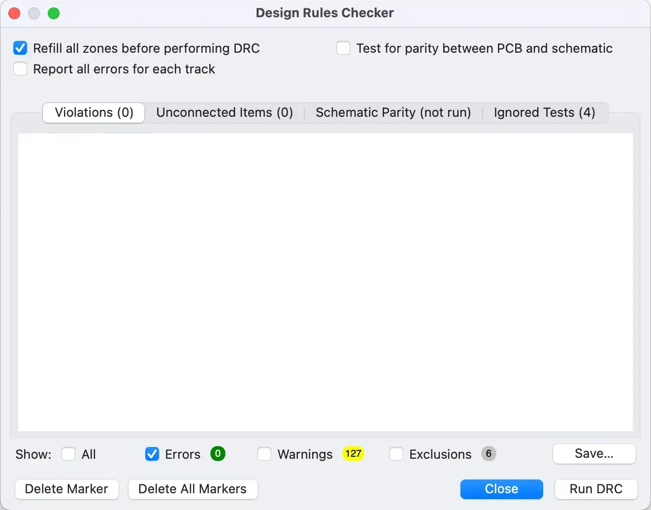
Running native DRC in KiCAD yielded several warnings related to component library syncing and silkscreen thickness, but no DRC errors. Woo!
Bring-up and validation
After receiving the assembled board from MacroFab, the primary functions I needed to validate as a part of bring-up were:
- Battery charging, including the behavior of onboard user and charge LEDs
- I2C communication via the exposed header pins using an external LCD
- Serial communication over USB to my computer
LEDs and LiPo charging
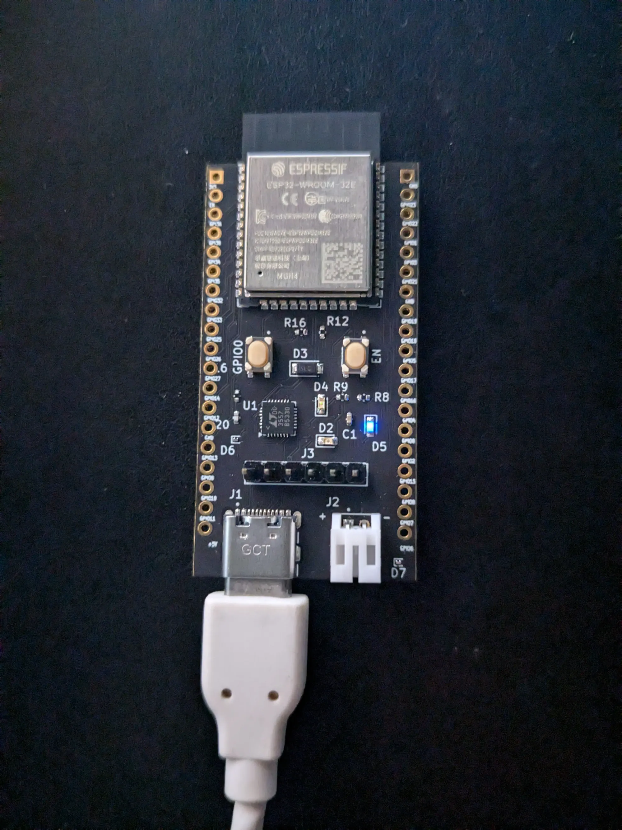
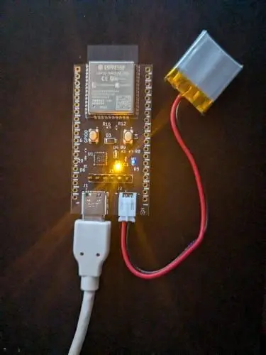
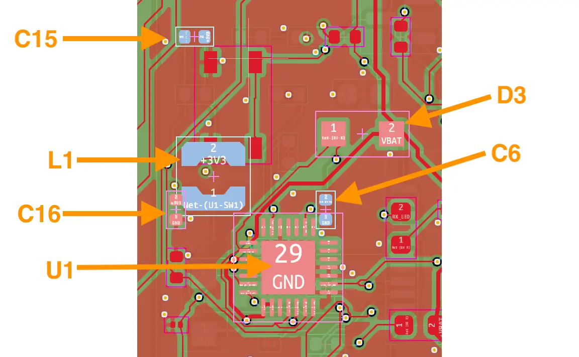
Image 6: QSP32 powers on and charges a single cell LiPo through power chip LTC3557
I validated the board's LEDs by programming a basic Arduino Blink example. This also demonstrated that the USB (5V) to 3.3V power regulation to the MCU was working sufficiently to allow programming through the USB-C to UART interface.
The active LED indicates a power source is connected and the LiPo battery is charging via the onboard LTC3557 IC. The battery shown here measures 3.9V.
All LEDs are functioning as expected, though the 20Ω resistor for the RX and TX LEDs could have been a lower value for increased brightness. Quilter and Macrofab correctly placed all diodes in the proper orientation. Kudos to Macrofab for their excellent work on this.
LCD via I2C
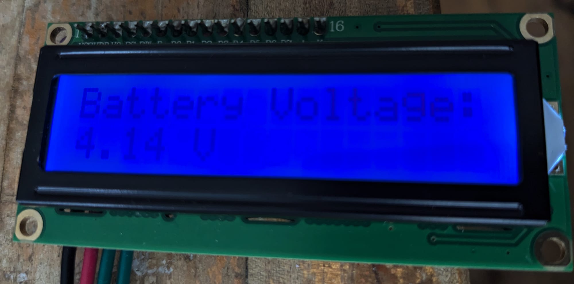
Hello World!
I wrote a quick Arduino sketch to display the battery charging voltage on an LCD via I2C. Though the LCD is slightly dim due to the 3.3V power supply (it's designed for 5V), it still displays the data clearly.
Serial
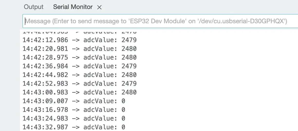
I'm using Arduino's serial monitor to debug a 12-bit analog-to-digital converter (ADC) through the USB-to-UART connection. The image shows ADC values when a battery is connected and when the ADC (GPIO35) is pulled to ground (adcValue: 0).
Design validation
With all the functional elements verified, let’s dig out the oscilloscope and take a closer look at the integrity of the QSP32’s most important signals.
Power
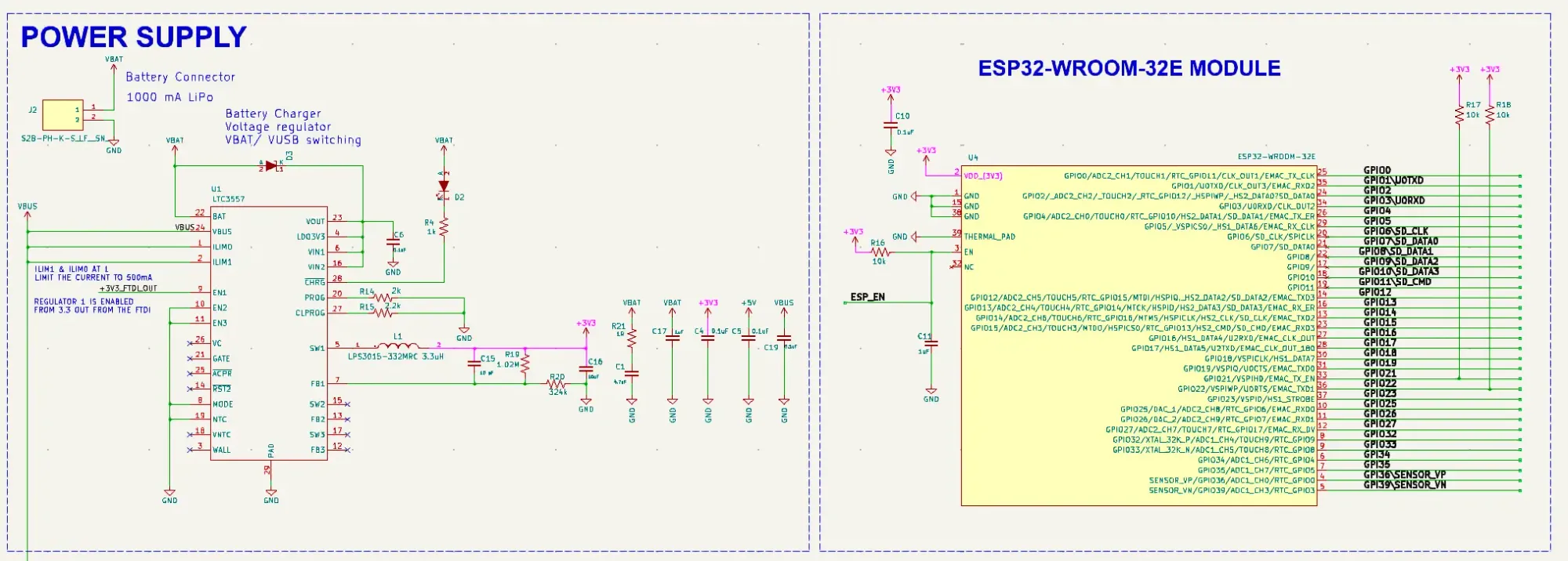
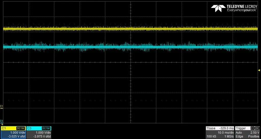
The QSP32's power input path starts with a USB-C connector, which feeds USB voltage through protection diode D1 to voltage regulator U1. U1's 3.3V output passes through an inductor, a capacitor, and a pair of resistors before reaching the ESP32 and a test point header some distance away.
The blue line shows the noisy input from the USB connector powered by my laptop. The yellow line represents the signal on the other side of protection diode D1, which also serves as the input to U1.
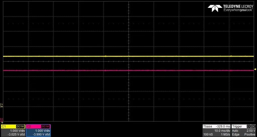
The 3.3V output from U1 is remarkably clean. The pink line on the oscilloscope represents this output. Further filtering occurs through an inductor, two capacitors, and two resistors, resulting in the final 3.3V supply. The yellow line shows a probe measurement at the ESP32's supply pin, demonstrating the effectiveness of this filtering.
Signal integrity: I2C
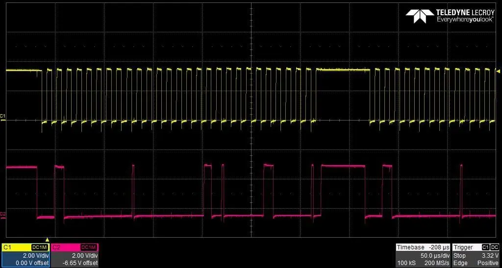
The I2C SDA (data) and SCL (clock) lines connect to a generic 16x2 LCD. To analyze these signals, I programmed the screen to refresh data every second. The oscilloscope displays the clock signal in yellow and the data in pink. I captured these signals by directly probing the ESP32's GPIO21 and GPIO22 pins.
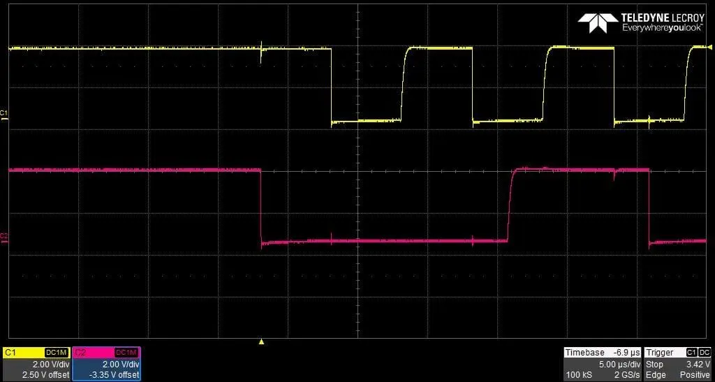
Here’s a closer look at these same signals:
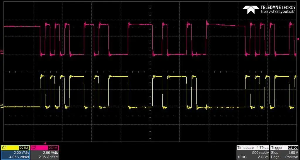
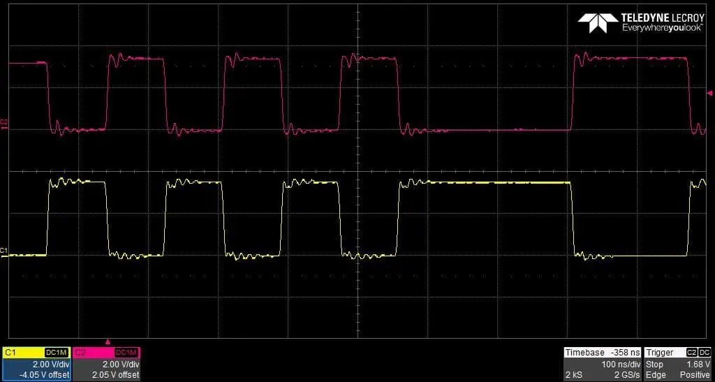
Signal integrity: USB
To assess USB signal integrity, I probed DP_N and DN_P at the USB-UART interface.
The DP and DN signals weren't well-matched in the layout because they weren't routed as differential pairs. While their characteristics are similar, they don't align perfectly (Image 16), potentially compromising signal integrity. This mismatch may increase noise susceptibility and cause phase shifts. In future iterations, proper differential pair routing will enhance overall signal reliability.
Despite this, programming the QSP32 via the USB-C connector is remarkably consistent and reliable. I fabricated three boards, and each one connects instantly.
Conclusions
I chose an ESP32 WROOM module because it integrates key components like the antenna, crystal, and bypass capacitors, which the Quilter team is still working on adding as physics constraints in the product.
In the future, we'll create an ESP32 module entirely with Quilter, and plan to incorporate the recent addition of differential pair support into the next revision of this design.
Quilter's automated placement and routing for this board performed exceptionally well, saving me several days of manual design work.
Design improvements
- Use Quilter’s Differential Pairs feature
- Add pull-down resistor on ADCs
- Configure LTC3557 to use battery power in addition to USB power
- TX/ RX LEDs are too dim
- Add power-on LED
- Remove unnecessary EN switch
- Replace the middle header with test points
- Add 5V output for LCD
- Make board in green for “prototype”
Next steps
Building on the QSP32 platform, I plan to co-design a digital audio mixer. This new design will feature rotary switches for volume control and an analog multiplexer (74HC4051) for routing audio signals.
Links/resources
- QSP32 project input files
- QSP32 project output files
- QSP32 source code