QSP32 Solar Boost
The QSP32 Solar Boost is a custom ESP32-based development board with an energy harvesting feature.
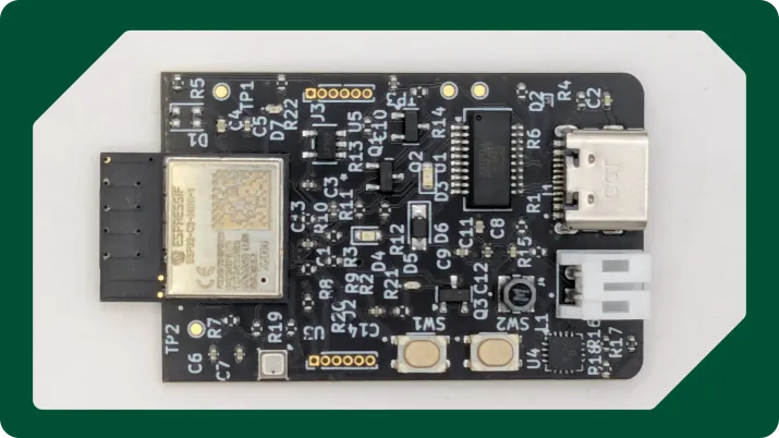
Building on the success of the QSP32, we’ve decided to push Quilter’s generative PCB designer into new territory — an IoT board that has an energy harvesting feature.
Meet the QSP32 Solar Boost!
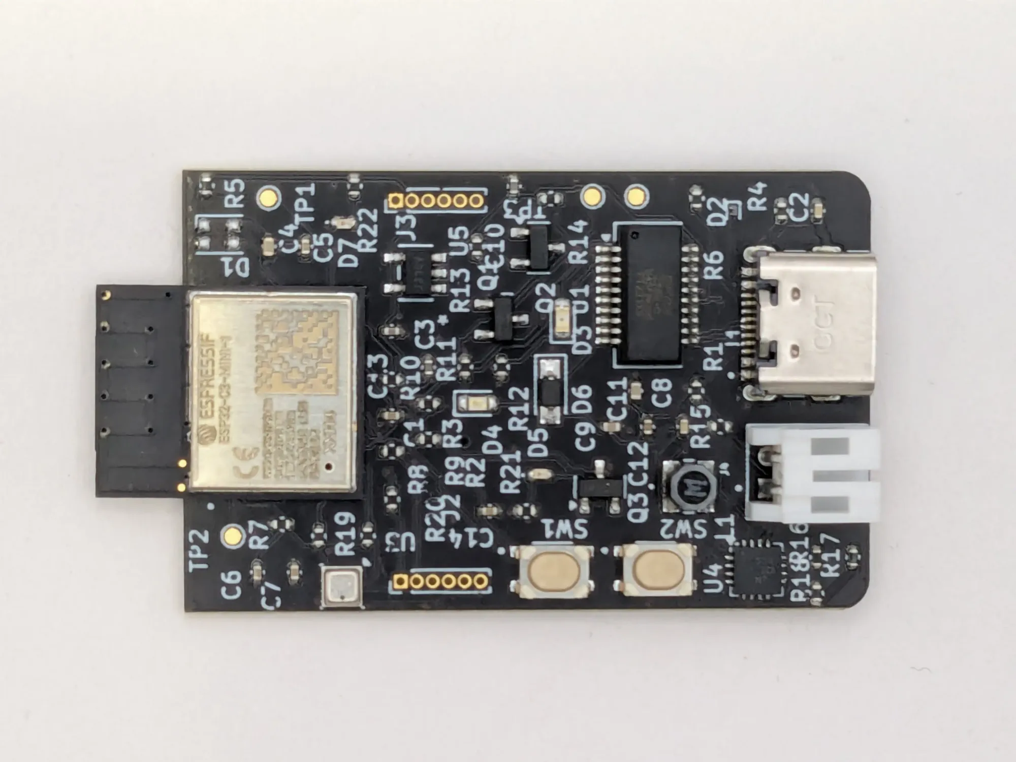
The QSP32 Solar Boost is a PCB designed to integrate solar powered charging into any IoT project. Just like the QSP32, this board layout was crafted entirely by Quilter’s generative design, without human intervention.
The QSP32 Solar Boost features the ESP32-C3-MINI-1 module plus:
- A USB 2.0 to UART chip,
- A 5V to 3.3V power regulating chip,
- A chip for energy harvesting micro or milliwatts from a solar panel,
- Access to GPIOs through headers,
- I2C interface for an LCD screen over i2C,
- A three in one package sensor for humidity, temperature, and pressure
Whether you’re optimizing for power efficiency or building eco-friendly devices, this project showcases Quilter’s ability to tackle real-world challenges while saving plenty of time.
TL;DR: Quilter did a great job with the layout, I had it made at Macrofab, and everything works as expected!
Read on for the complete project write-up!
QSP32 Solar Boost blinking Hello World
Designing with Quilter
Configuring a job in Quilter happens in two high-level steps:
- Uploading input files (schematic and board file) that define the netlist, component footprints, board outline, and position of any pre-placed components.
- Defining constraints that identify the primary physics concerns for Quilter’s AI designer to respect during layout.
Input files
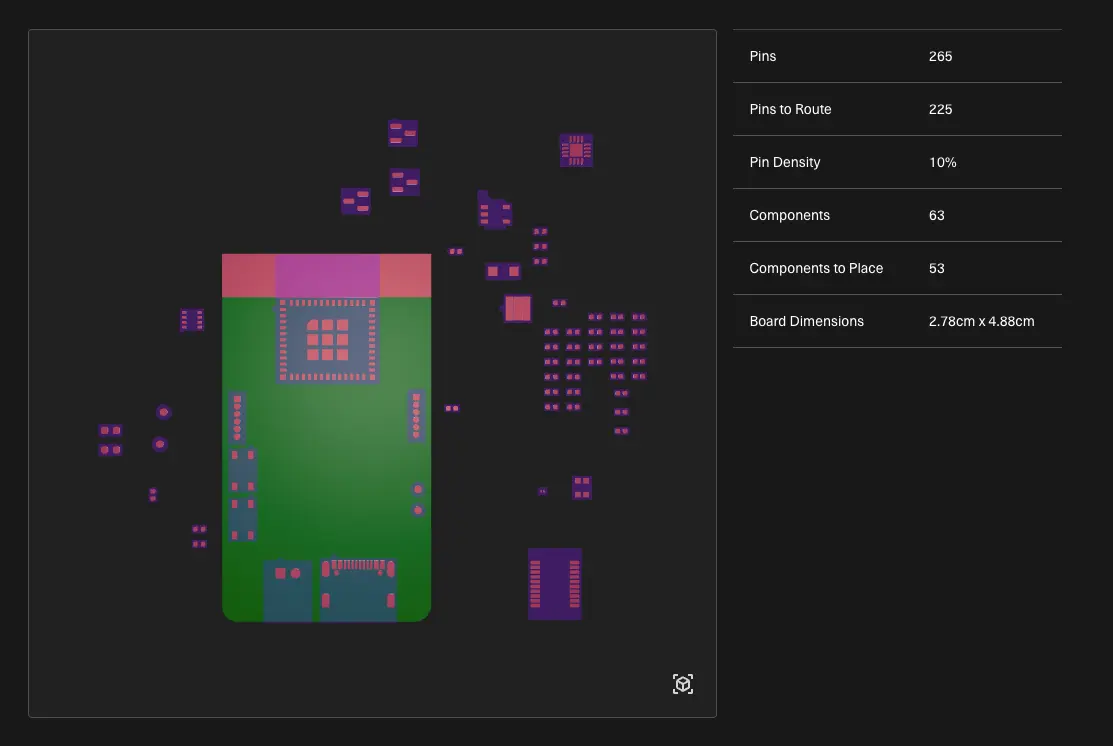
I pre-placed a few location-sensitive components in this design:
- The ESP32-C3-MINI module because I wanted to ensure the ESP32 trace antenna extends off the edge of the board to reduce signal interference.
- USB and battery connectors: I grouped these together along a common edge.
- Push buttons: These were placed in close proximity to the ESP32 for accessibility.
- Solder points for the solar panel: I am exploring how they will integrate with an enclosure.
The rest of the components were left unplaced for Quilter to handle. On the right, you can see that there were 63 components in total – I pre-placed 10 components, leaving 53 comps with 265 pins left for Quilter to place and route.
Physics constraints
For the QSP32 Solar Boost, the primary physics considerations for my designs were:
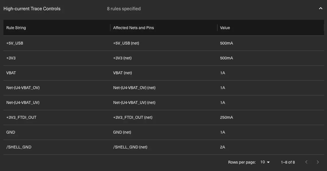
- High current nets for the USB-C power supply and Li-Po charging circuitry
- Differential pairs to deliver USB signals between the USB-C connector and UART
- Bypass capacitors to ensure adequate decoupling and filtering
Here are the high current net constraints I defined before submitting my layout job to Quilter.
Quilter now has a Differential Pairs feature! Although differential pairs are only required for high-speed, noise sensitive communication protocols such as Ethernet or USB, I defined one set of differential pairs on the USB-to-UART (USB to serial) bridge to test the feature.

Output file
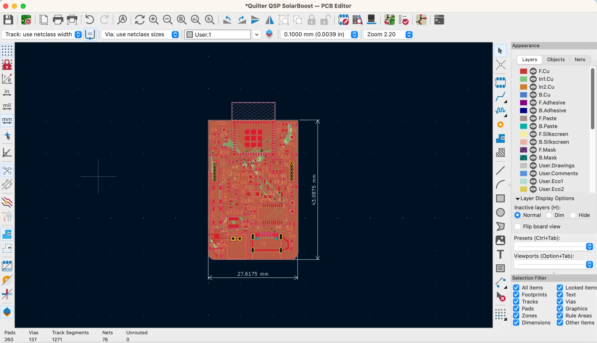
Two hours after uploading my input files, I chose Candidate 7 out of 12 candidates because it met my preferences for a single-sided layout, 4 layers, and choice of fabricator.

Here’s the design I chose.
Bring-up and validation
After receiving the assembled board from MacroFab, the functions I needed to validate were:
- Voltage regulation: a stable 3.3V for the ESP32
- Energy Harvesting via solar panel
- Serial communication over USB to my computer
- I2C communication via the exposed header pins using an external LCD
- Sensor data over I2C: pressure, temperature, humidity
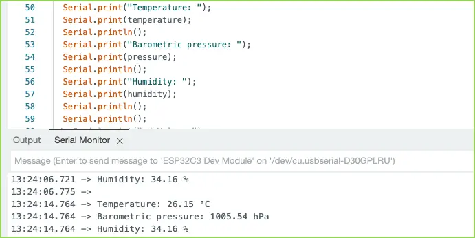
I validated the Solar Boost voltage regulation, serial communication, and BME280 sensor operation in one move - by programming a BME280 sensor data collection sketch into the ESP-C3-MINI module.
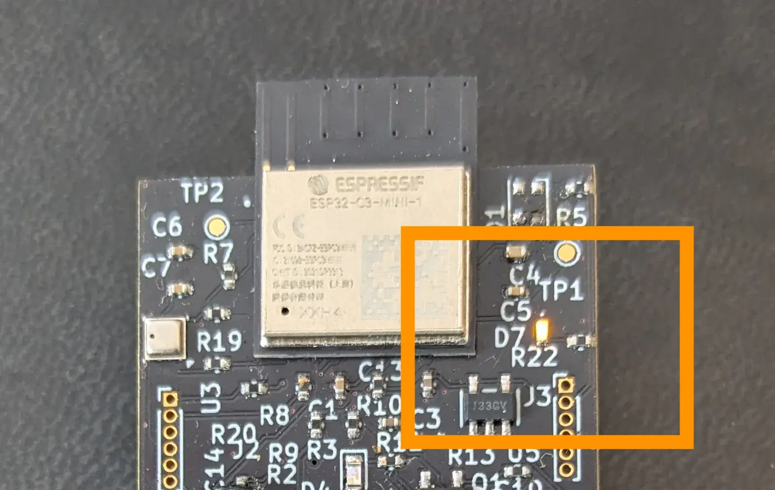
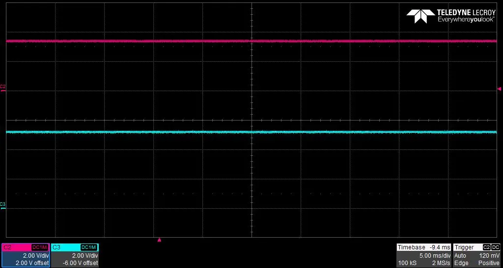
Programming and reading data serially in the second image below indicates that the voltage regulator is regulating a stable 3.3V (from 5.2V USB power) to the ESP32. For additional validation, there’s a power on LED (D7) between 3.3V and ground shown directly below.
Energy Harvesting
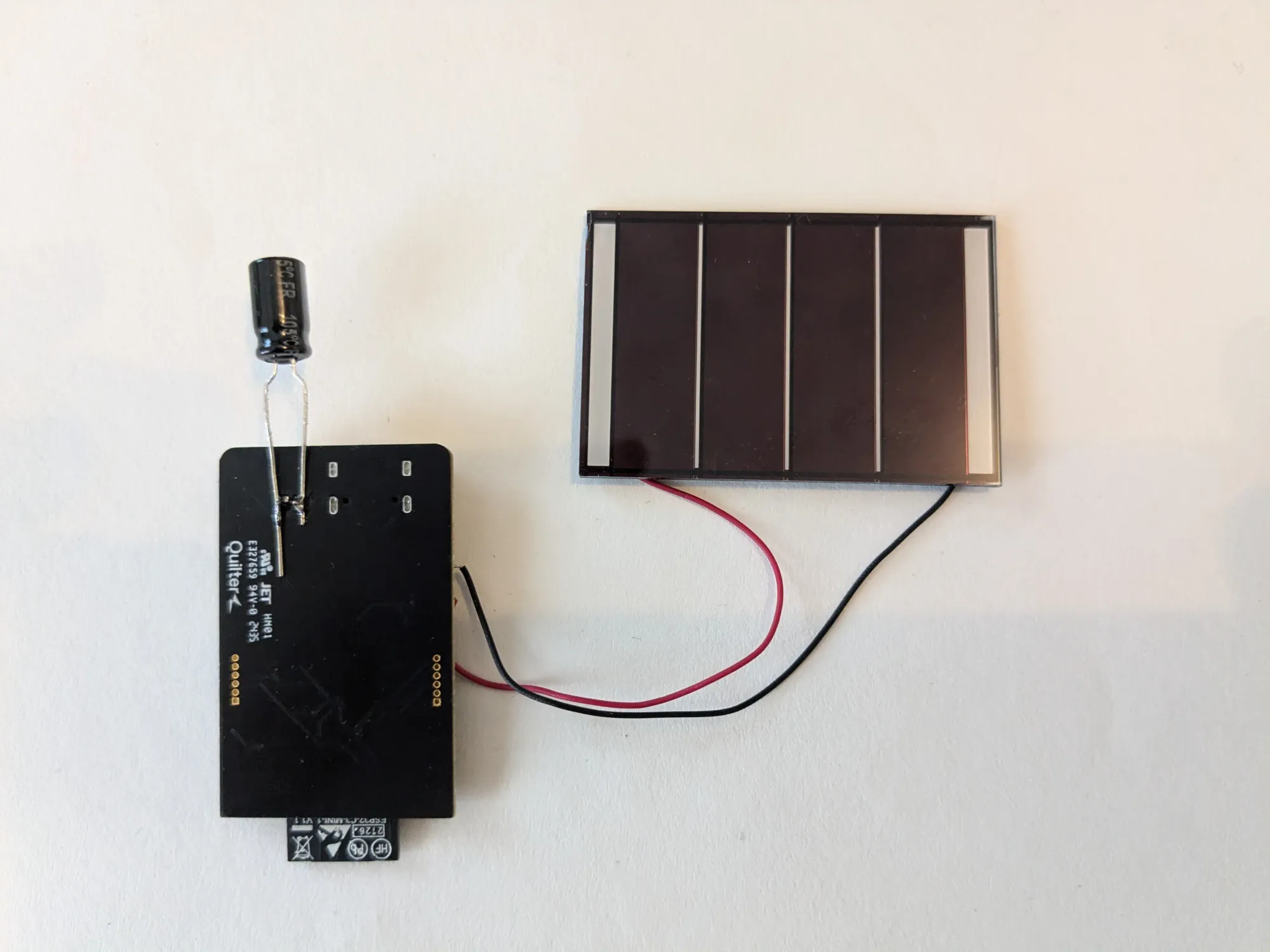
Energy harvesting happens through the BQ25504: a boost converter designed to acquire and manage micro or milliwatts generated from devices like a solar panel. I validated functionality with a small (~1.25” x 2”) solar panel with an open circuit rating of 3.4V and 2.2V maximum power point (V @pmpp) and a 470uF polarized capacitor rated for 6.3V.
I placed the probes on the capacitor while moving the panel in and out of sunlight. The capacitor charges and discharges rapidly and although this video is sped up by 1000X you can see the signal clearly.
The QSP32 Solar Boost charging and discharging a capacitor via a solar panel
LCD via I2C
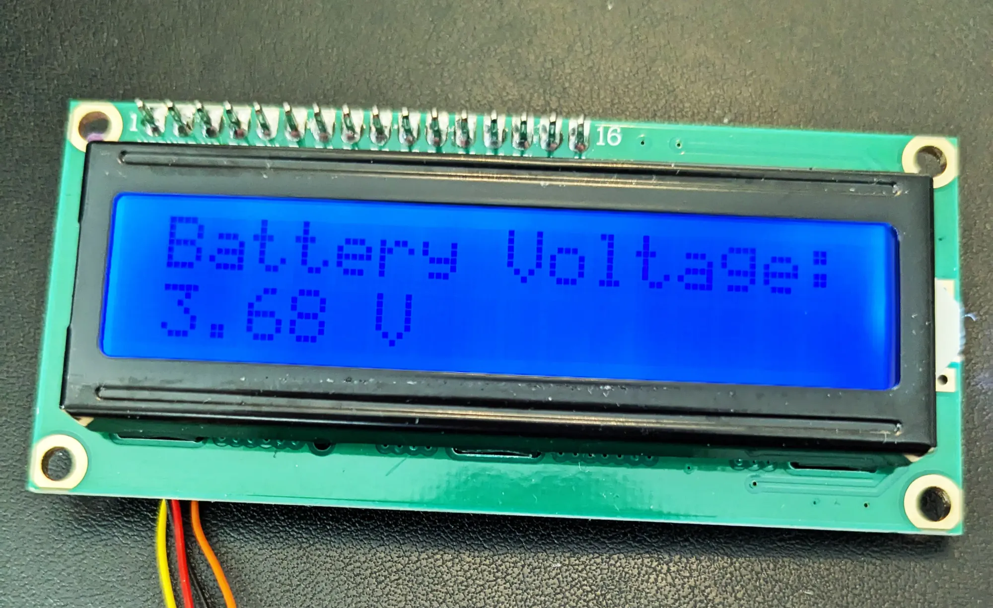
This LCD is connected to exposed header pins on the Solar Boost PCB to display real time data transmitted via the I2C bus.
I programmed a simple sketch to read and display battery voltage, confirming that the PCB layout is functioning correctly.
Design validation
The QSP32 Solar Boost is working perfectly!
Now that we’ve validated its functionality, let’s take a closer look.
Signal integrity: Differential Pairs
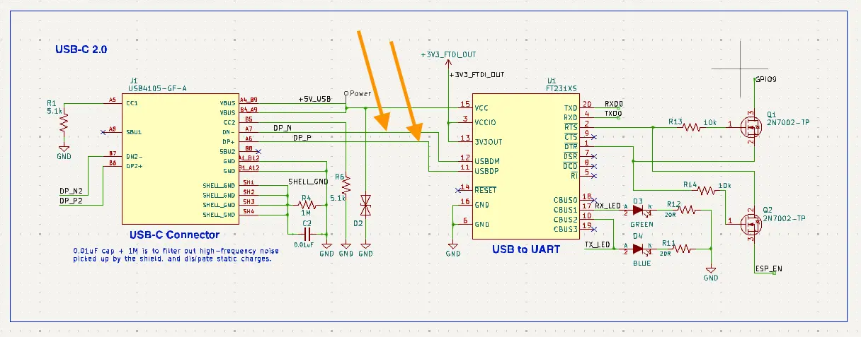
Quilter is adding new features all the time and since Quilter now supports differential pairs,
I used the feature to support the traces between USB and UART (orange arrows). As discussed above, the USB-to-UART bridge does not require this feature, but I enjoyed testing it regardless.
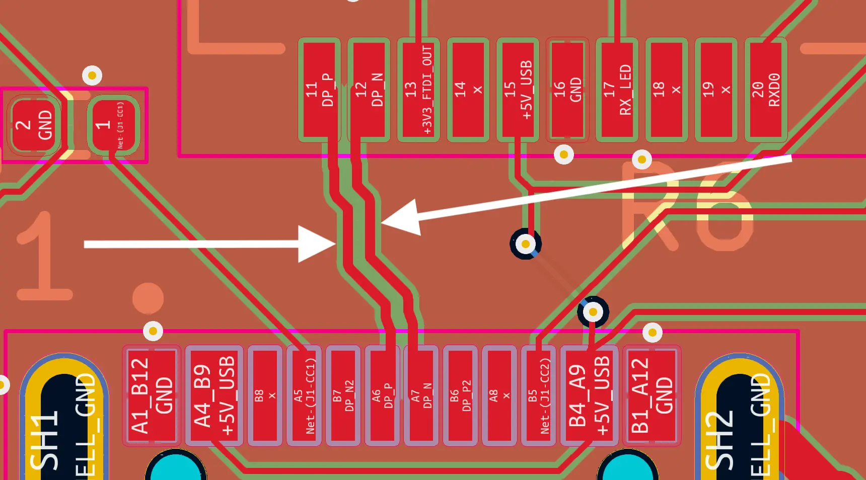
Quilter did a great job of placing the FTDI chip close to the USB-C connector. These traces go between a UART chip (top) and a USB-C connector (bottom). The layout of the differential pairs has precise length matching for good signal integrity.
I put probes on DP_P and DP_N (white arrows).
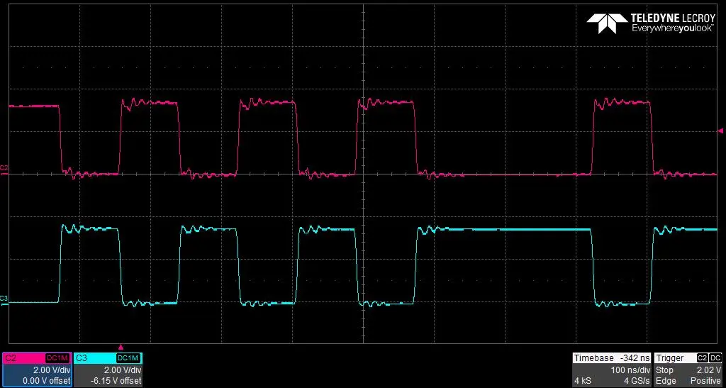
This oscilloscope capture displays the differential signals from the USB to UART interface, with the red (DP) and blue (DM) traces showing opposite polarity as expected. The signals are clean and show a consistent signal integrity.

The closeup of these differential pairs looks excellent! There's no noise, and the signals are perfectly mirrored.
Power regulation
The QSP32 Solar Boost power path starts with USB power (5.2V) via a USB-C connector. The USB power path goes to a 3.3V voltage regulator and is regulated down to 3.3V. ESP32s require very stable power to operate, so the regulator needs to do a good job.

Most regulators require bypass capacitors on the input and output to stabilize the voltage supplied to the regulator, for decoupling, as filters for high-frequency noise, and for transient response when the load on the system increases or changes.
Here’s how Quilter both placed and did the layout for the Solar Boost’s voltage regulator with its input and output capacitors. If I were hand placing these components myself, I would follow the datasheet’s instructions.
Set external components, especially the output capacitor C13, as close as possible to the ICs, and make wiring as short as possible.
That said, this didn’t seem to matter as the voltage measures a quite stable 3.3V everywhere that I could reach on the board.
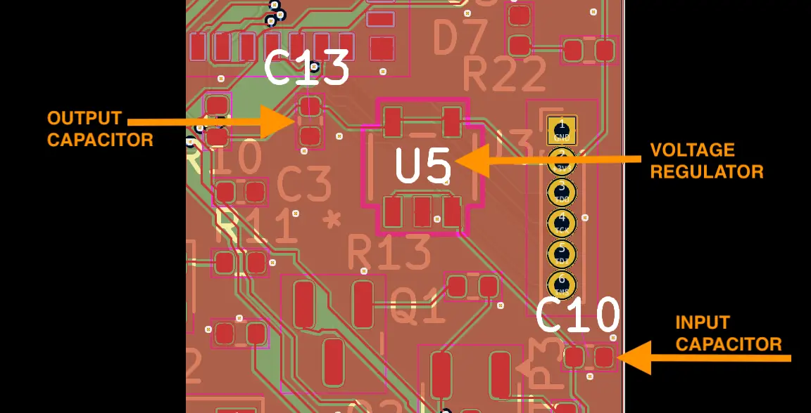
One month after the Solar Boost was fabbed, Quilter now handles bypass capacitors through our “Circuit Comprehension”.

The blue trace in this oscilloscope screenshot represents the voltage on the 5V line from the USB-C connector, while the red trace shows the 3.3V output from the voltage regulator. The 3.3V output is very clean, showing the effectiveness of the filter.
Signal integrity: I2C
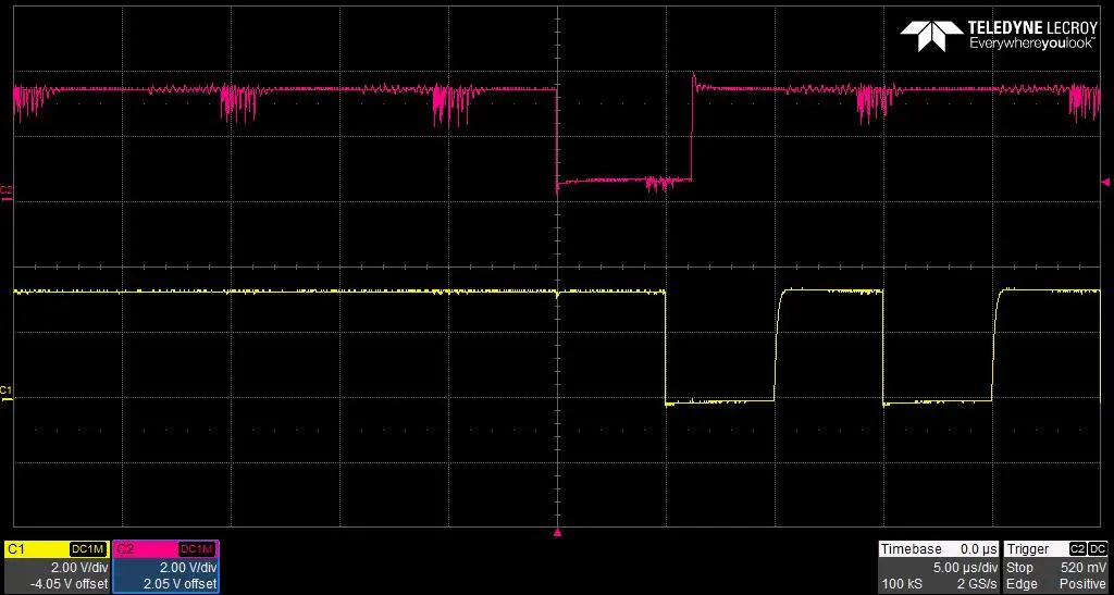
Two devices, the LCD and the trio of sensors, are communicating over this bus at the same time. I captured the SDA (data, red) and SCL (clock, yellow) clock signals while both devices were running. Although the signals look a little noisy, this is likely because the LCD screen is attached by fairly long (3”) hookup wires.
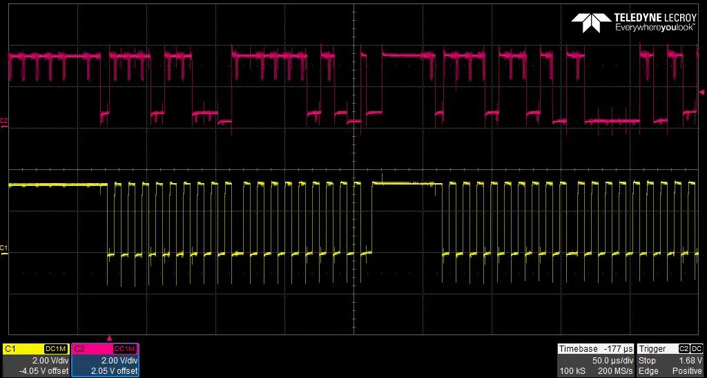
Not initializing the sensors via software on the I2C bus didn’t make much difference (not shown), but physically removing the LCD screen made the signal less noisy.
This is not surprising as I mentioned above - the LCD screen is attached to hookup wires that connect to external pads on the board.
1. I2C is a robust communication protocol that can tolerate noise
2. You can optimize a PCB all you want, but signal integrity can (and does) get impacted by off-board concerns!
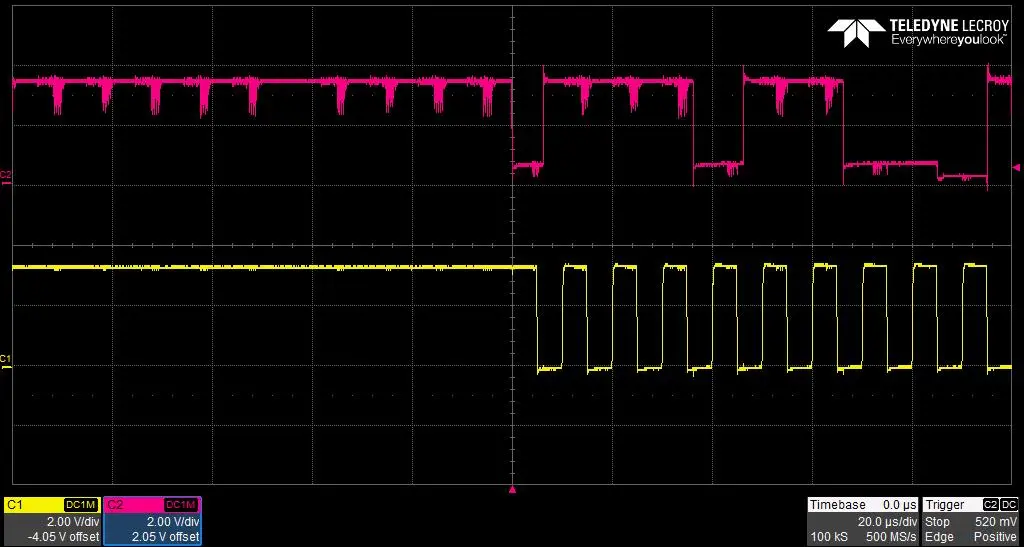
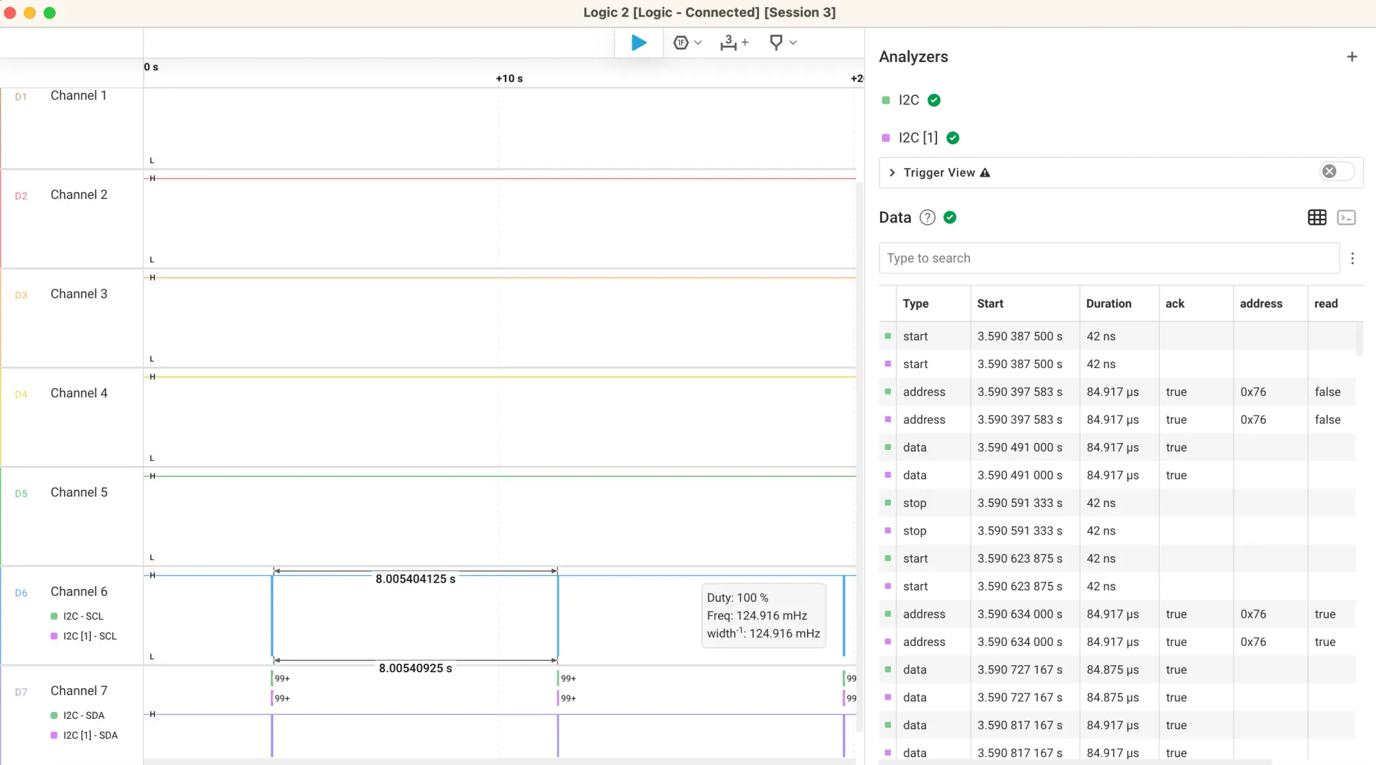
For fun, I used a Saleae logic analyzer to poke at this signal. We can see the address of the sensor 0x76 and an 8-second delay that I programmed into the sketch. Unsurprisingly, the logic analyzer correctly recognizes these signals as I2C!
Conclusions
I chose the ESP32-C3-MINI module because it integrates essential components such as the antenna, crystal, load capacitors, and bypass capacitors. As Quilter adds more features, I’m looking forward to designing a complete ESP32 module using Quilter.
The next revision of the QSP32 Solar Boost will also have bypass capacitor functionality! Quilter's automated placement and routing for this board worked really well, saving me several days of manual layout.
Design improvements
- Tie both sides of USB-C connector together for reversible input
- Pulldown resistor on ADCs
- Configure to operate on battery power in addition to USB power
- GPIO0 incorrectly wired to Q1
- Fix D1 4 pin footprint to use as RGB status
- Reverse D6 (backwards in design)
- Remove D5 because energy drain
- Review configuration resistor values on BQ25504
- Remove unnecessary EN switch
- Solar panel relocation
- Make board in green for “prototype”
Next steps
Building on the QSP32 Solar Boost, I’ll work on improving its efficiency for use in low-power solar applications. It would be a sweet little product that could be used in all kinds of low-power climate data capture with an enclosure, a smaller LCD screen and a better mechanical fixture for the solar panel.
Links/resources
- QSP32 Solar Boost input files
- QSP32 Solar Boost output files
- QSP32 Solar Boost Arduino sketch


