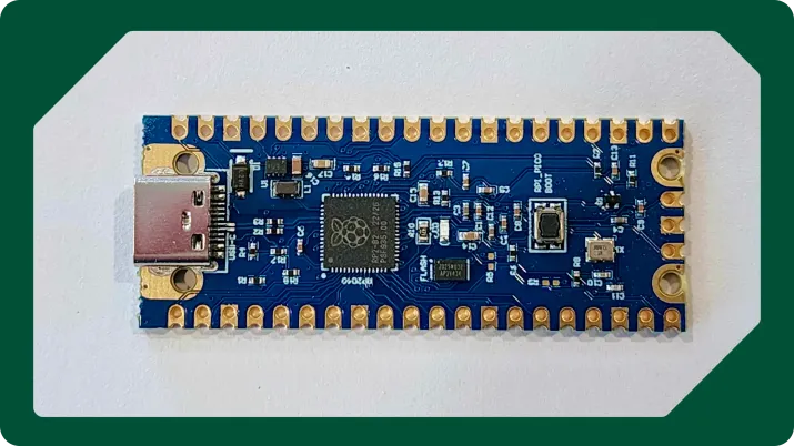
Quilter is home to several example designs based on open-source hardware, one of which is a “clone” of the popular Raspberry Pi Pico. We call this example “Qpico”.
It’s one thing to have a completely placed and routed board document, but the real proof of the pudding is in the eating as they say - so I looked through the 100% placed and routed candidates from a compilation run and selected one to build and bring up.
Original Design Credit
First, I want to give credit where credit is due: This project is based on the open-source “AvocadoPi” - a Raspberry Pi PICO variant with USB Type-C connector, as shared by designer Sindre Hovland on GitHub.
This in turn was based on the original Raspberry Pi PICO by Raspberry Pi Ltd, creators of the RP2040 microcontroller. It’s nicely designed and includes high-quality footprints with 3D models.
TL;DR: Quilter's Qpico design fabricated and assembled by JLCPCB boots fine.
Here is the result: a set of fully assembled blue Pi Pico's with USB-C host connectors, routed 100% by Quilter:
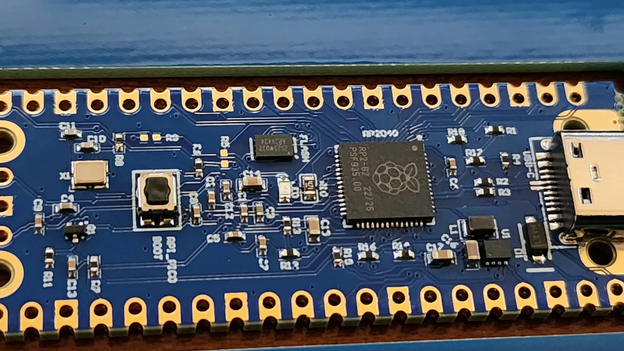
Loading the obligatory “blink” from the Raspberry Pi PICO SDK examples:
Qpico Project Details
Qpico is slated to become one of our “instant examples”. Given that Raspberry Pi Ltd. has recently released the next-generation dual-core microcontroller (the RP2350), you can be sure I’ll be spinning up a new version with the new chip as soon as I can get samples. For now, the RP2040 is still a very cool platform for so many projects!
This version of Qpico is straightforward:
- RP2040 Microcontroller (Dual ARM Cortex-M0+)
- USB Type-C host interface
- USB VBUS to 3.3V switching regulator
- 16 Mbit QSPI Flash for program (and non-volatile data storage)
- An ultra-bright green LED on GPIO25
- Various supporting components for clock, bypassing, and boot.
The original point of this design is to improve the Pi Pico with a USB Type-C host connector since it’s superior (by a long margin) to the original’s USB micro-B type. Given that Quilter now supports diff-pairs, routing the USB 2.0 is trivial for this kind of board - even through series termination resistors.
I made some slight alterations to Sindre’s original schematic to make the results a bit faster and remove a couple of bottlenecks for Quilter. Let’s explore those a bit. If you want to follow along, you can view or download the files here.
Schematic Modifications
The original official Raspberry Pi PICO design includes a few test points that provide access to the USB DP/DM pair, as well as LED (GPIO25), GPIO23, the QSPI SS pin, and, of course, GND.
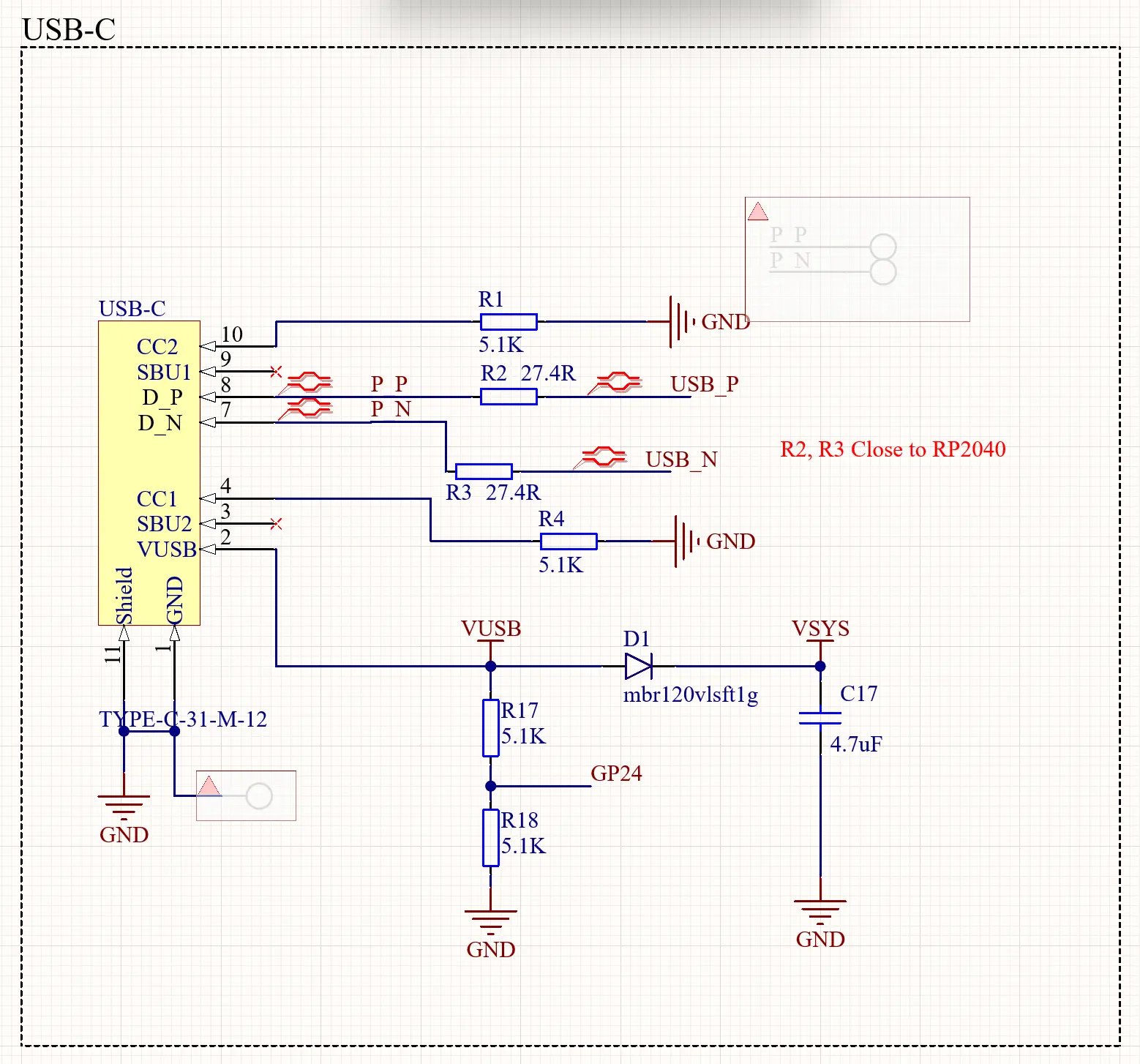
I don’t intend to use or require any of those, so the first thing I did was cover all the test points on the schematic with “Compile Masks” in Altium - this prevents the objects under the masks from being placed or included as footprints on the PCB document. The example below shows the mask covering the USB pair test points:
USB-Type C Footprint Hack & Pre-Placed Parts
Also, you might look at that USB connector symbol twice - and recognize that pins 5 and 6 are missing from the regular pin sequence. That’s because I modified the symbol and footprint for the USB type C connector.
As you probably know, USB Type C allows the cable to be plugged in right-side-up or upside-down. For USB Type-C, the center pins on top and bottom form the reversible D_P and D_N pair. Normally, this means that the USB 2.0 diff pair has to be routed to both pairs of pins on the top and bottom of the connector - which, in turn, requires a cross-over. The screen-shot below is the way Sindre had originally done it - and the vias on the diff pair lead to the bottom layer where the test points are:
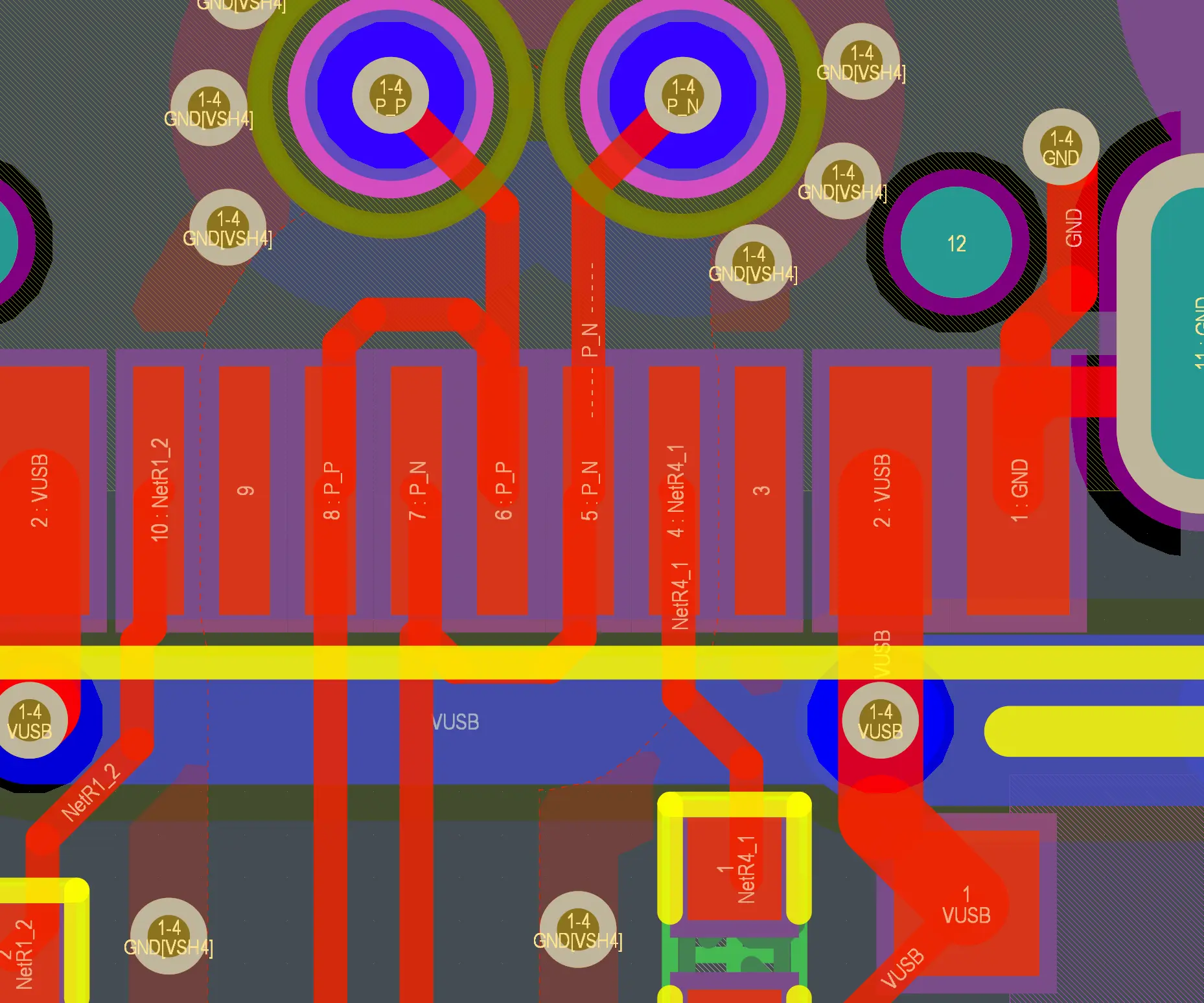
While Quilter does now support diff pairs, we’re still working on training it to do these more complex structures and layer changes, so at the time of this writing, I simply re-created the footprint for the USB-C connector with the reversing connections as a built-in part of the footprint - and it works perfectly!
Here’s the footprint:
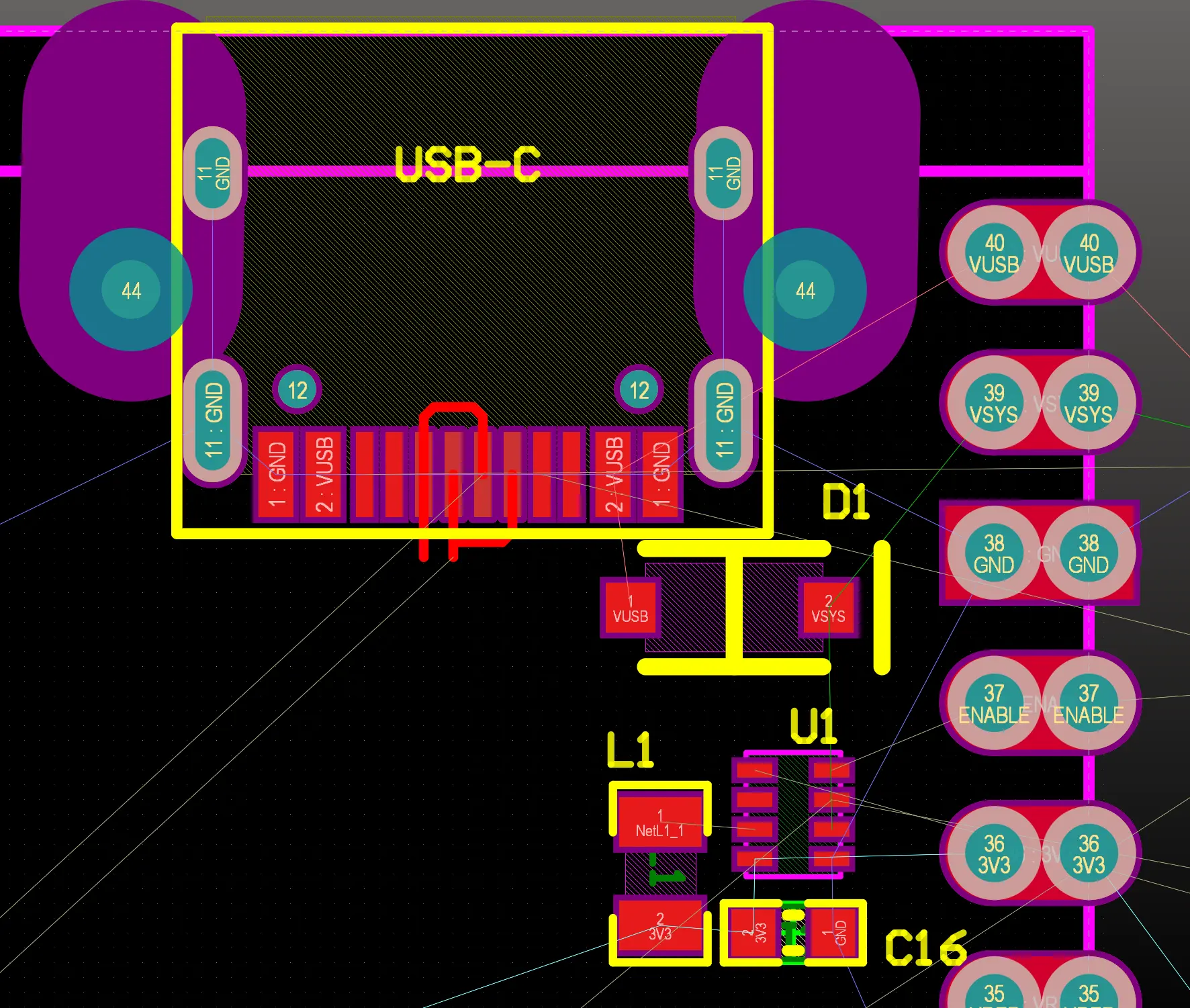
Notice also - I deliberately pre-placed the input protection diode D1, and the buck voltage regulator (U1, with L1 and C16). This pre-placement helps control how Quilter will route this power supply, keeping current loops between U1, inductor L1, and output capacitor C16, small.
The USB-C connector and the 40-pin “DIP” castellated edge module footprint, of course, were also pre-placed in keeping with the original dimensions and pin-out of the Raspberry Pi Pico.
Quilter Inputs and Constraints
Input files
Before uploading the Altium source documents, I made sure there were no other synchronization issues between the schematic and PCB. With the critical pre-placement of the Pico castellated module (J1), the USB C connector and buck regulator, everything else was ready to be done.
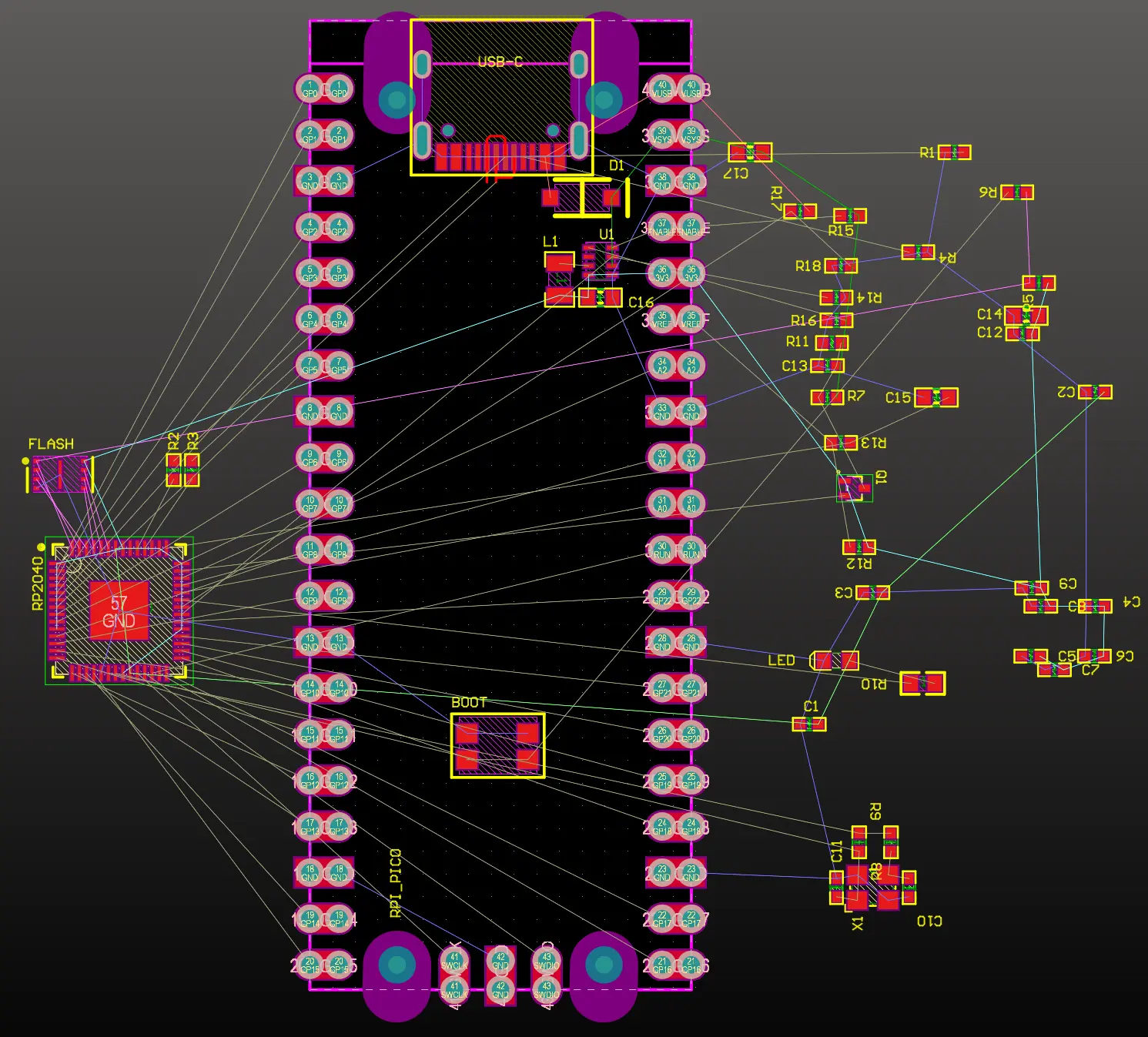
I also pre-placed the BOOT pushbutton as seen above in the Altium Designer PCBDoc. I didn’t make any changes to the source file Design Rules since Quilter will re-assign rulesets for each layer stack and fabricator automatically.
Designing with Quilter
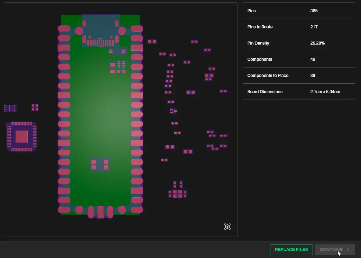
The Qpico PCB with the pre-defined placement was uploaded into the Quilter app - a quick visual check shows the pre-placed USB-C connector is good to go:

Physics constraints
With the PcbDoc and SchDoc files uploaded to a new layout job in Quilter I then setup the routing constraints as follows:
- High Current Net (width) rules:
VBUSVBUS→ 500mA (USB spec)VSYS→ 500mA (VBUS through the protection diode)NetL1_1→ 300mA (the buck regulator switching node to the output inductor L1)3V3→ 300mA (used to power the GPIOs as well as the FLASH memory)1V1→ 200mA (Internal CPU core power supply)*
- Differential Pairs:
P_P:P_N→ 85-OhmsUSB_P:USB_N→ 85-Ohms
USB specifies differential impedance in the interconnect between 75 and 100-Ohms, but in general sticking to 85 or 90 is best for good signal integrity.
Output file
Once Quilter completed the job there were several 100% completed candidates to choose from. I selected Candidate 56, as I filtered the results based on using 4-layers and vias with a minimum hole size of 10mil, and minimum clearance of 5mil. This configuration is suitable for Macrofab but can be used with most other quick-turn PCB manufacturers as well. The 2 inner layers in this case are GND, so all the signal traces are microstrip lines.
I downloaded Candidate 56 and added the PCBDoc to my original Altium Designer project. Here are the top and bottom layer copper view for reference:
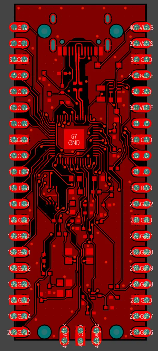
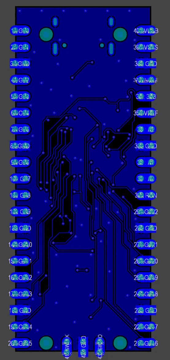
Top (left) and bottom (right) view of result after polygon repour.
I use the Altium Designer command Report » Measure Distance to do a few quick checks around the board - especially for the 85-Ohm differential pair dimensions and clearance. These match the impedance calculation that was done for the layer stack defined in Quilter - so everything is correct.
Even though the differential pair trace width and spacing is calculated for a specific target impedance that depends on a specific layer stack, I’m not super concerned with the variation in this case (if any variation exists) because the RP2040 chip only supports USB 1.1 speeds (12Mbit/s) and the USB specification for version 1.1 compliance is broad: differential impedances from 75-Ohm to 120-Ohm are allowed.
Design validation & cleanup
Although this design has met layer stack and manufacturing clearance constraints, there are a few things that need to be cleaned up before going to production:
- GND polygons on signal layers contain several unconnected “islands”.
- Silkscreen (legend) texts and items are not placed and need a human touch.
- Some Solder Mask sliver areas are too narrow.
Executing a Design Rule Check in Altium Designer on the candidate board reveals these issues:
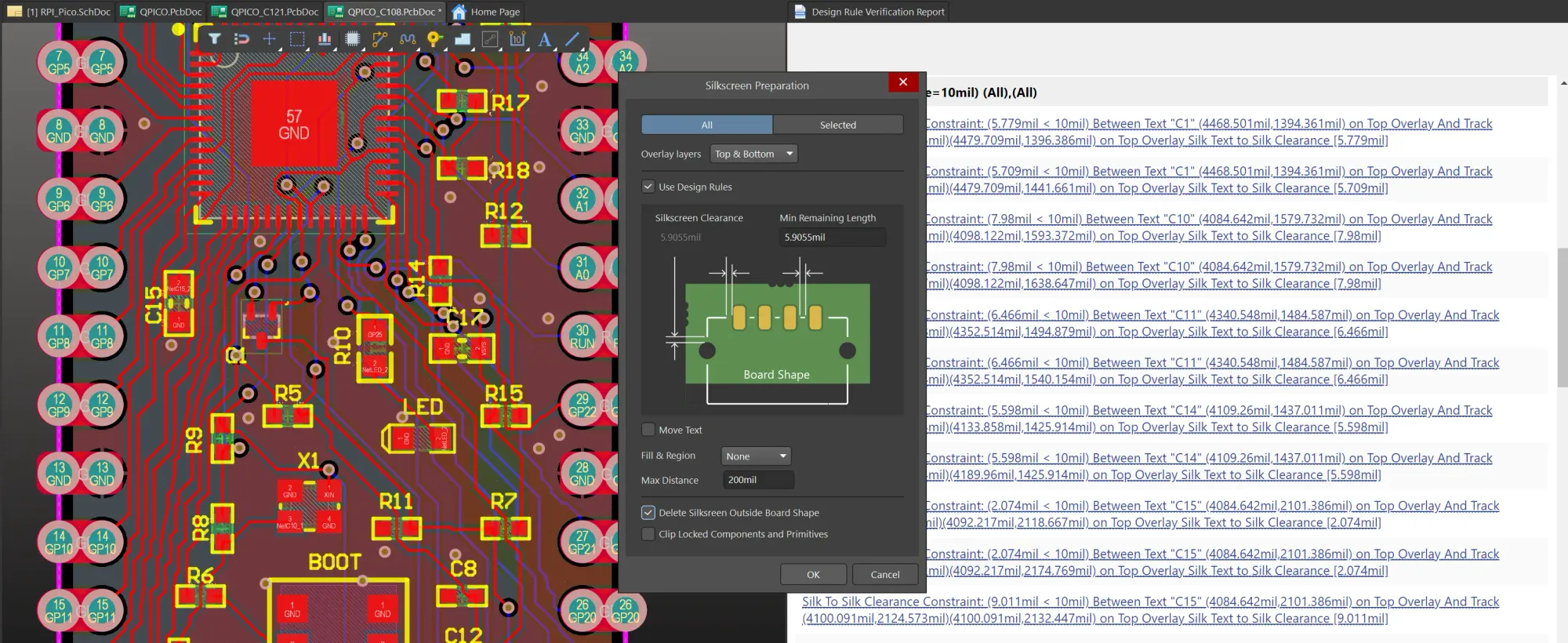
Thus, I manually relocated pretty much all the silkscreen texts (component designators) and also “cheated” by relaxing the default silkscreen clearance and solder mask sliver design rules a little bit. I also updated the design rule for Solder Mask Expansion to be 0 mils - this means that for any component pad, the solder mask will be right up against the edge. While this relies on theoretically perfect registration of the images in the fab shop, the reality is that the fabs these days will typically be happy with this and make slight modifications if necessary.
I also had to update Altium Designer’s clearance rules to have additional clearance for the differential pair. Although Quilter already cleared the pair according to the impedance profile, the polygon clearances were not added to the PCB design rules. Re-pouring the polygons will remove that impedance control gap.
Oh, I also added the Quilter logo on the bottom layer silkscreen and “Qpico” in text.
After adding these minor changes and finishing clean-up, the DRC in Altium Designer clears with zero errors:
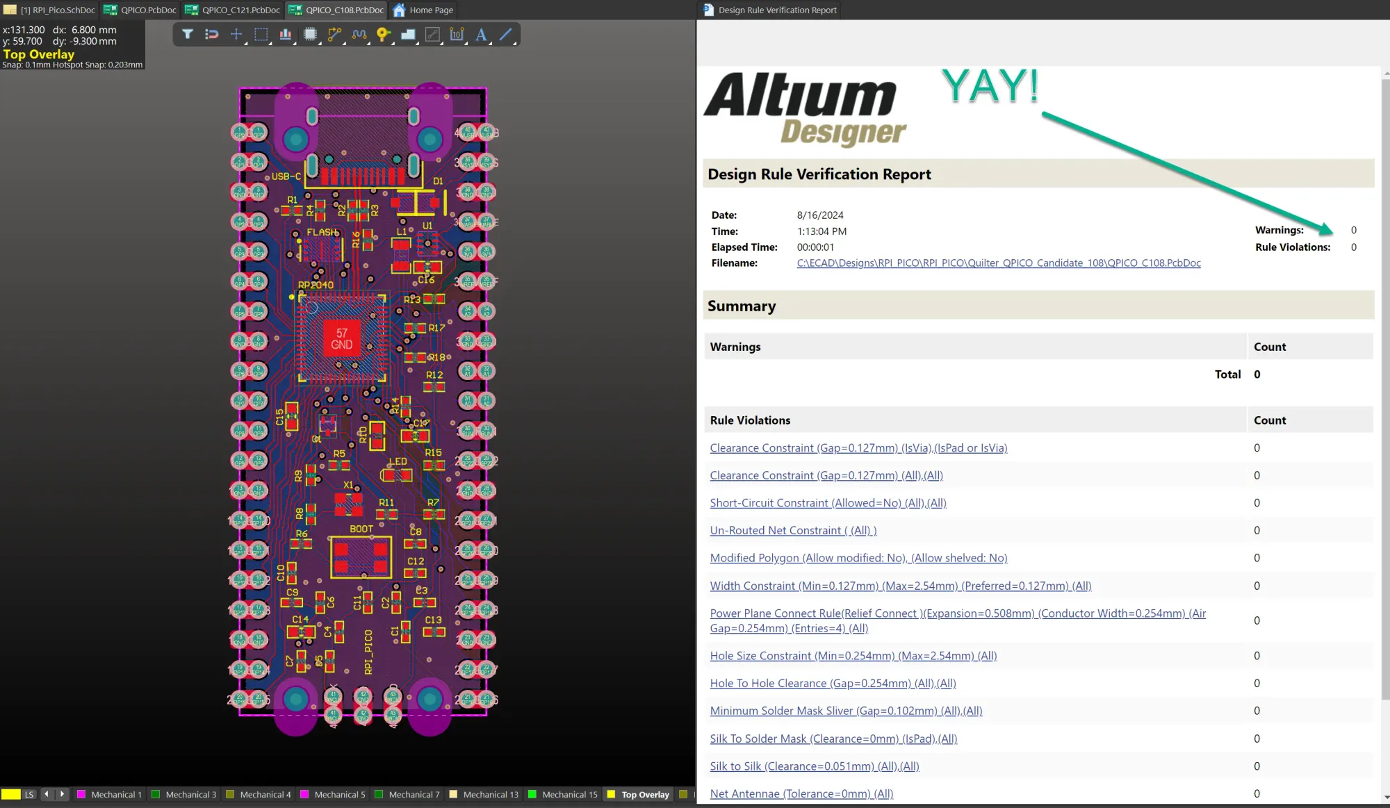
Now it’s ready to go to manufacturing.
Getting Qpico to Fab
The original plan was to have this fabricated by our friends at Macrofab, using their standard 4-layer service. During the process of scrubbing the parts list (BOM) I hit a few snags:
- The USB Type-C connector is not readily available in US inventory (though it’s widely available in Asia).
- The RP2040 microcontroller is not in stock at the most common US-based distributors (it’s more commonly directly sold by Raspberry Pi Ltd.)
- The source design specified a 2016-sized crystal. But 12MHz is the required frequency for the RP2040 chip, and 2016 is physically too small to fit a 12MHz crystal.
Unfortunately, that 3rd point meant I had no choice but to modify the crystal footprint to be 2520 sized; luckily, that was able to be done without touching the actual routing of the board as the 2520 crystal package fits in exactly the same spot with enough room around it, and without having to move any traces. The only thing required was to repour the top ground polygon. DRC is still a pass.
Macrofab offered to consign the parts for the RP2040 chips and the USB-C connectors, which necessitated me ordering them from Asia and waiting for shipping before sending them for the kit to Macrofab. I didn’t want to wait that long, so I decided to try JLCPCB for this run.
JLCPCB was a little more convoluted regarding organizing the assembly because I chose to use a new service they offer where I paid $10 extra to have them select suitable generic components for the resistors and capacitors on the board. So I waited about a day and a half, and when they’d completed that step, all I had to do was re-order the board with assembly service, at which point I uploaded the simply formatted parts list and pick-and-place CSV files.
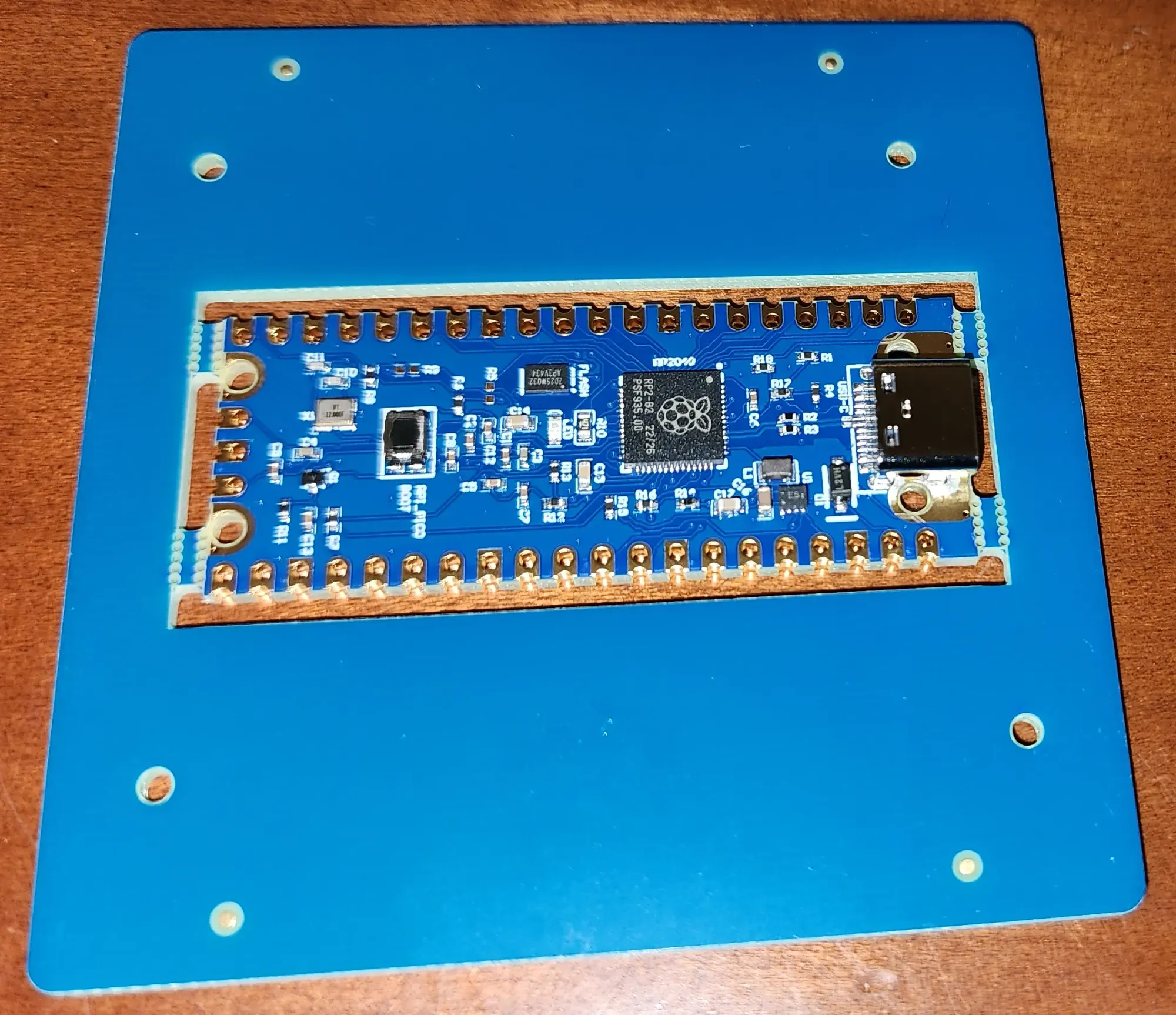
Then on to a quick validation of the parts list - again having to specify just the USB-C connector and RP2040 SKUs from their LCSC supply web site. That done, I was off to the races as they say. Within a week and a half I have the fully assembled Qpico boards in hand:
Bring-up and validation
I am a little impatient, but knowing that this board design originated with the Raspberry Pi Pico, which is well-known and well-tested, and having thoroughly reviewed the schematics for correctness, I was confident there would be no issues.
So, I exercised the first board (I ordered 10) and plugged it into my host PC via USB-C. I was rewarded with the familiar “new device found” Windows sound, as well as the tray notification that a new USB drive had been connected - M: (RPI-RP2). Yay!!
Power
Even though I used reasonably large constraints for trace currents, the calculator still allows them to be fairly narrow for 20°C temperature rise. Moreover, the constraint current of 500mA is way more than this board and microcontroller will ever actually use. The RP2040 datasheet shows a full-utilization of a single core draws a bit less than 18mA. With both cores at full utilization, the current draw will never exceed 40mA - so a constraint for the 1.1V core supply of 200mA is overkill (and I did that deliberately to make sure the trace width didn’t go too narrow for my liking).
That said, the DC-DC converter that provides the 3.3V board supply is doing it’s job nicely and also powering the external 1.8” TFT display and it’s backlight quite nicely.
TFT Example
Just to show we can run something more elaborate than the “blinky” project, here’s a library example that uses the ST7735S TFT display driver. This one uses the SPI 1 interface - a hardware SPI peripheral in the RP2040 with dedicated clock and data I/O pins.
The source code for the ST7735S display demo is downloadable from https://github.com/bablokb/pico-st7735-demo - credit to bablokb for providing this resource.
I used the hardware SPI 1 interface pinout, which is defined in the makefile for the demo project:
# library configuration (override if necessary, see pico-st7735 for a complete list)
set(SPI_TFT_PORT "spi1" CACHE STRING "TFT spi port-name")
set(SPI_TFT_CS   "9"    CACHE STRING "TFT CS  pin number")
set(SPI_TFT_DC   "10"   CACHE STRING "TFT DC  pin number")
set(SPI_TFT_RST  "11"   CACHE STRING "TFT RST pin number")
set(TFT_OPTIONS TFT_ENABLE_BLACK TFT_ENABLE_RESET TFT_ENABLE_TEXT TFT_ENABLE_SHAPES
                TFT_ENABLE_ROTATE TFT_ENABLE_SCROLL
            CACHE STRING "TFT options/functions")

#program configuration
set(SPI_PORT "spi1" CACHE STRING "spi port-name")
set(SPI_RX   "12"   CACHE STRING "RX  pin number")
set(SPI_TX   "15"   CACHE STRING "TX  pin number")
set(SPI_SCK  "14"   CACHE STRING "SCK pin number")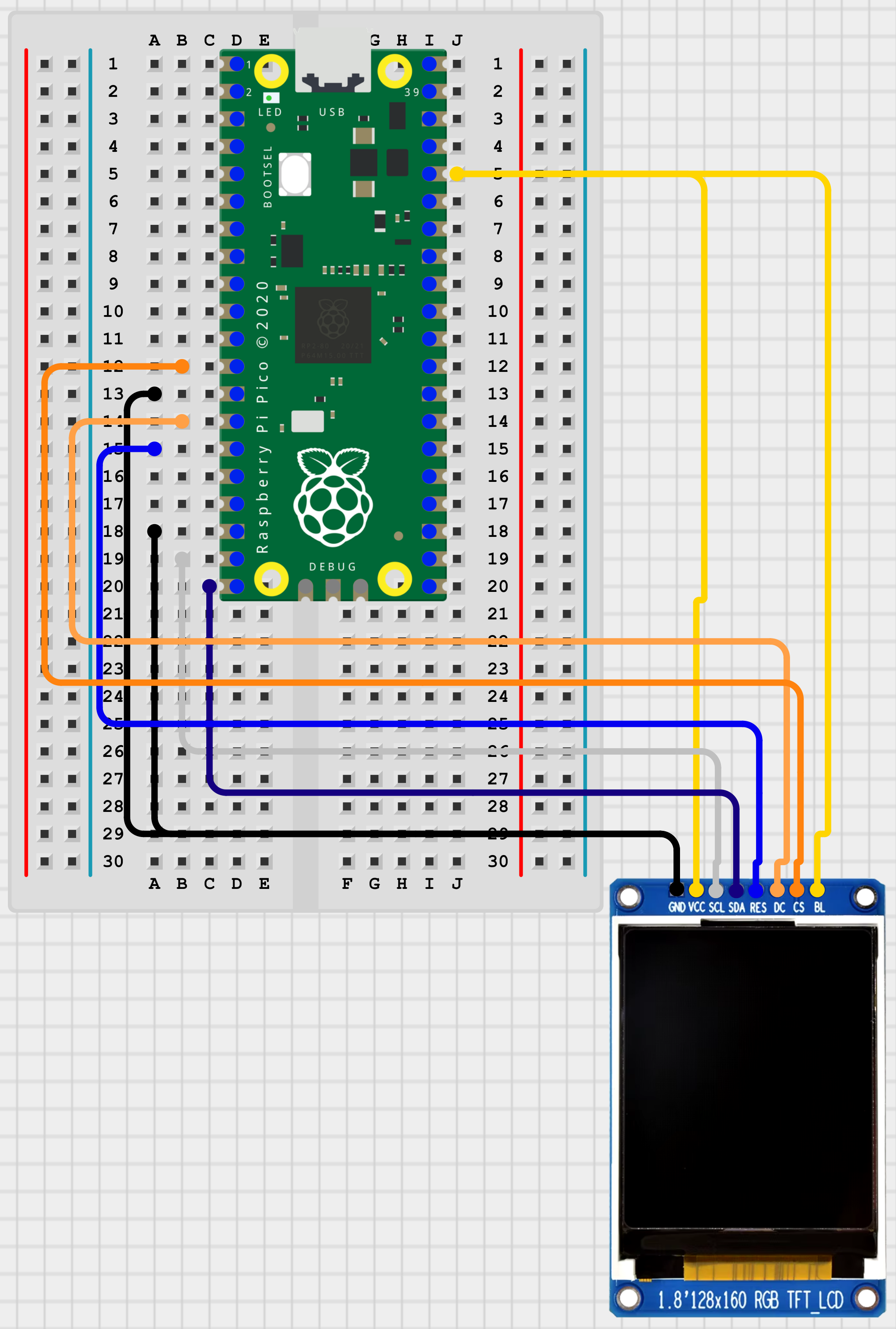
This Circkit Designer diagram is essentially what’s on my breadboard.
All that, and I’m good to compile the code in my Pico Dev Container. To save time, you can download the UF2 program files from the test examples below.
When you plug in the Pico board while holding down the BOOT pushbutton (or any Raspberry Pi Pico for that matter), it appears as a mass storage drive. Just drag and drop the desired UF2 file into that drive to program the board and it will automatically reboot and run the firmware.
Conclusions
It has occurred to me through this process how easily I can use Quilter as a “custom breadboard” tool as well. For many digital electronics projects I undertake, I loath the thought of starting with a traditional breadboard and tons of “Dupont” wires.
Though it’s often the only solution to test out a basic circuit within a short time frame, I’d much rather use Quilter and a quick-turn prototype service. And I still get vastly superior signal integrity given the inner ground planes, than with the breadboarding approach. It’s also going to be a lot less prone to errors or bumping the wires with my stubby fingers.
Design improvements
This design suffered the only roadblocks around parts availability. For the next one, I’ll be updating to use a widely available 2520 sized crystal, a more common pushbutton for bootloading mode, and an alternative USB Type-C connector which can be obtained from US suppliers as well as those in Asia.
Next steps
This overall works really well. I’m now almost in possession of the new Raspberry Pi RP2350 sample kit, so stay tuned as I’ll be back with a fresh new design of the QPICO2, based on the RP2350 dual ARM Cortex-M33 / Dual Hazard3 microcontroller.
Resources
Here are the archived resources exactly as I used to build the boards with JLCPCB as well as the test firmware and related Raspberry Pi RP2040 documentation.
Altium Project:
JLCPCB BOM and Pick-n-Place
UF2 Firmware Test Files


